
Reactor used for semiconductor single crystal material vapor phase epitaxy growth

A technology of single crystal material and vapor phase epitaxy, which is applied in the direction of polycrystalline material growth, single crystal growth, crystal growth, etc., can solve the problems of growth thickness and thickness uniformity difference, low pass rate, interference with crystal growth, etc., to ensure Effects of epitaxial growth rate, residence time extension, and conversion rate assurance

Active Publication Date: 2016-10-05
SINO NITRIDE SEMICON
View PDF10 Cites 2 Cited by
  • Summary
  • Abstract
  • Description
  • Claims
  • Application Information

AI Technical Summary

Problems solved by technology

[0003] At present, the reactor structure in the HVPE system generally has the problem that the epitaxial growth rate gradually slows down with the consumption of the metal source, which leads to poor repeatability of the process. The height of the liquid level of the liquid metal source is different), and the growth thickness and uniformity of the thickness obtained under the same process conditions will be significantly different
The fundamental reason is that the reactor structure of the HVPE system at this stage cannot guarantee that the probability of converting halide gas or halogen gas into metal-containing precursors is basically the same when the metal source liquid level is at different heights, so that the consistency of the flow field cannot be guaranteed.
As a result, the group III nitride single crystal material grown by HVPE technology has poor consistency and low pass rate, which seriously hinders HVPE technology from being used in large-scale production.
At the same time, a small amount of unconverted metal source vapor will be transported to the growth area or the substrate surface with the carrier gas, forming polycrystals and interfering with crystal growth, causing microcracks or lattice distortion in the epitaxial crystal, which greatly reduces the crystal growth. Quality and Product Yield

Method used


Image

  • Reactor used for semiconductor single crystal material vapor phase epitaxy growth
  • Reactor used for semiconductor single crystal material vapor phase epitaxy growth
  • Reactor used for semiconductor single crystal material vapor phase epitaxy growth

Examples


Embodiment 1

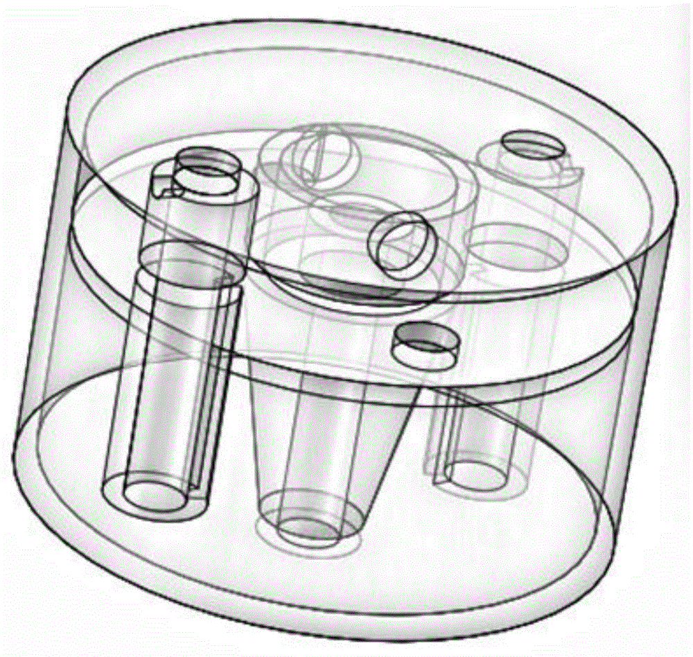
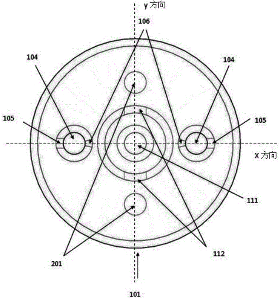
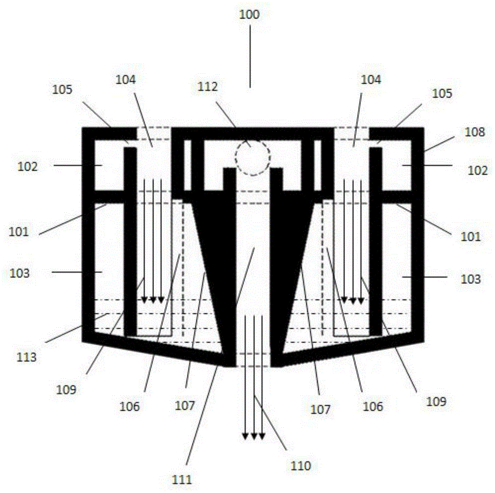
[0025] The reactor 100 for vapor phase epitaxy provided by the present invention (such as figure 2 , image 3 , Figure 4 (shown) includes: a baffle 101, an air inlet pipe 104, an inverted trapezoidal circular platform 107, a first air outlet 201, a second air outlet 112, a metal-containing precursor output pipe 111, and a reactor outer wall 108;

[0026] The baffle 101 divides the reactor into an upper space 102 and a lower space 103; two circular first air outlets 201 are arranged symmetrically on the baffle 101; the halide gas or halogen gas reacts with the metal source to generate a metal-containing precursor Objects 110 flow into the upper space 102 through the air outlet 201; two air intake pipes 104 extend from the upper space 102 to the bottom of the lower space 103. The size of the inner diameter of the air inlet pipe 104 can be determined according to the requirements of the process; the air inlet pipe 104 is connected with an external gas source, and the metal so...


PUM


Abstract

The invention provides a reactor used for semiconductor single crystal material vapor phase epitaxy growth. The reactor is composed of a baffle, gas inlet pipes, an inverted-trapezoidal truncated cone, gas outlet holes, a metal-containing precursor outlet pipe, and an outer wall. The baffle divides the reactor into an upper-layer zone and a lower-layer zone. Openings are provided at the tops of the gas inlet pipes, such that part of halide gas or halogen gas is preserved at the upper-layer zone of the reactor, and can be subjected to a reaction with a metal source steam escaped from the lower-layer zone to the upper-layer zone. Therefore, the metal source is effectively prevented from mixing into a reaction precursor, and quality and yield of crystals obtained through epitaxy growth are greatly improved. Also, with the inner side wall openings of the gas inlet pipes, the baffle, the inverted-trapezoidal truncated cone and the gas outlet holes, halide or halogen gas flow direction and process can be changed, such that the retention time of the halide or halogen gas in the lower-layer zone is increased. The chance for the halide or halogen gas to contact the metal source is increased, such that the efficiency for the halide or halogen gas to be converted into the metal-containing precursor is not sensitive to the height of metal source liquid level. Therefore, conversion efficiency is stable; epitaxy growth rate and crystal quality are stable and controllable. The reactor facilitates the large-scale production of nitride single crystal materials.

Description

technical field [0001] The invention relates to the field of semiconductor material equipment, in particular to a reactor for vapor phase epitaxial growth of semiconductor single crystal material. Background technique [0002] Group III nitride semiconductor materials (such as GaN, AlN) and their compounds have excellent properties such as large band gap, high thermal conductivity, high pressure resistance and corrosion resistance. They are used in high temperature, high frequency, high power electronic devices and high brightness and high power LED / LD has a huge application prospect. Chemical vapor deposition (CVD, including MOCVD and HVPE) is currently the main method for the epitaxial growth of Group III nitride semiconductor materials. In particular, the hydride vapor phase epitaxy (HVPE) technology has become the mainstream method for growing single crystal GaN materials due to its fast growth rate and simple process. In HVPE technology, halide gas or halogen gas (su...

Claims


Application Information

Patent Timeline
Patent Type & Authority Applications(China)
IPC IPC(8): C30B25/08C30B25/14C30B29/40
Inventor 何进密刘南柳李文辉张国义
Owner SINO NITRIDE SEMICON
Learn More