Manufacturing method of BiCMOS integrated circuit

A manufacturing method and integrated circuit technology, which is applied in the field of device manufacturing, can solve the problems of small reverse withstand voltage of devices, and achieve the effect of improving reverse withstand voltage and increasing the maximum working voltage

Inactive Publication Date: 2016-10-05
PEKING UNIV FOUNDER GRP CO LTD +1
View PDF8 Cites 4 Cited by
  • Summary
  • Abstract
  • Description
  • Claims
  • Application Information

AI Technical Summary

Problems solved by technology

[0006] The invention provides a method for manufacturing a BiCMOS integrated circuit, which is used to solve the problem that the reverse withstand voltage of the device is relatively small due to the existing BiCMOS integrated circuit manufacturing method

Method used


Image

  • Manufacturing method of BiCMOS integrated circuit
  • Manufacturing method of BiCMOS integrated circuit
  • Manufacturing method of BiCMOS integrated circuit

Examples


Embodiment Construction

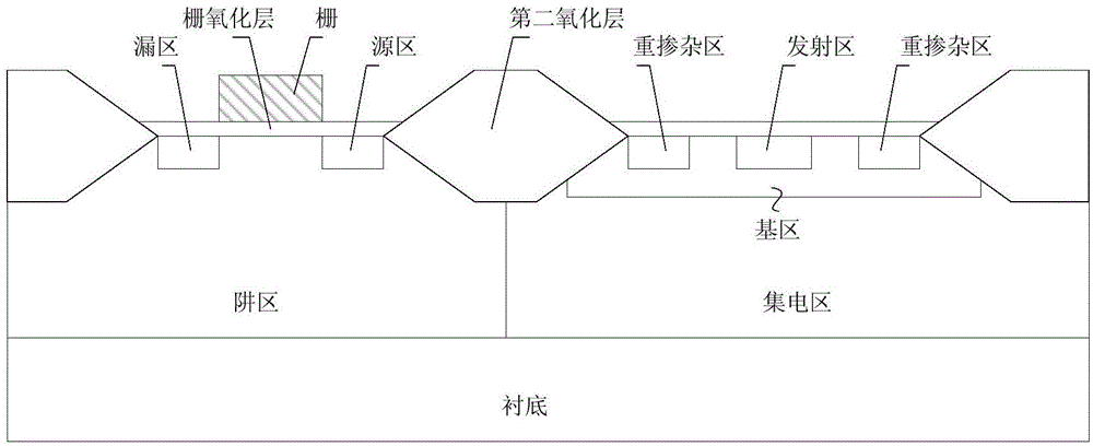
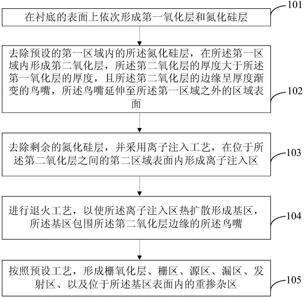
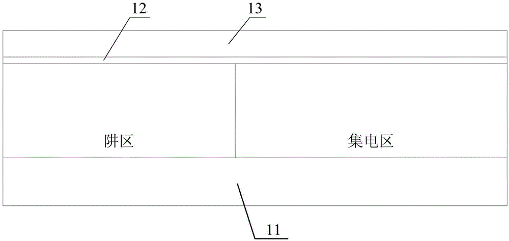
[0022] In order to make the purpose, technical solutions and advantages of the embodiments of the present invention more clear, the technical solutions in the embodiments of the present invention will be clearly and completely described below in conjunction with the drawings in the embodiments of the present invention. For convenience of description, the sizes of different layers and regions are enlarged or reduced, so the sizes and ratios shown in the drawings do not necessarily represent actual sizes, nor do they reflect the proportional relationship of sizes.

[0023] The semiconductor manufacturing process is a series of process steps implemented on the semiconductor wafer, including photolithography, ion implantation, annealing, oxidation, growing thin film layers, dry etching, wet etching, etc. The semiconductor wafer is a wafer-shaped semiconductor The substrate of the material. Semiconductors include single crystal silicon and polycrystalline silicon. Doping impurity e...


PUM


Abstract

The present invention provides a manufacturing method of a BiCMOS integrated circuit. The method comprises a step of orderly forming a first oxide layer and the silicon nitride layer on the surface of a substrate, a step of removing the silicon nitride layer in a preset first area, forming second oxide layers in the first area, wherein the edges of the second oxide layers are in the shape of a beak with increasing thickness, and the beak extends to the area surface outside the first area, a step of removing the remaining silicon nitride layer and forming ion implanting area in the second area surface between the second oxide layers, a step of carrying out annealing process such that the ion implanting area is allowed to be in thermal diffusion to form a base area which surrounds the beaks of the edges of the second oxide layers. Through the scheme provided by the invention, the base area can laterally spread to an area under the beaks and surrounds the beaks, when a transistor is under high voltage, a wide depletion layer can be realized in the base area, thus the reverse voltage withstanding of the BiCMOS integrated circuit is improved, the highest working voltage of the transistor is raised, and the requirement of a high voltage device is satisfied.

Description

technical field [0001] The invention relates to the field of device manufacturing, in particular to a method for manufacturing a BiCMOS integrated circuit. Background technique [0002] BiCMOS is an integrated circuit that integrates a bipolar transistor (Bipolar) and a complementary metal oxide field effect transistor (CMOS) in the same chip. It has the advantages of high integration and low power consumption of CMOS, and has the high-speed , The advantage of strong current drive capability. [0003] The existing method for manufacturing BiCMOS integrated circuits includes: forming a well region and a collector region in the surface layer of the substrate, and then growing a first oxide layer on the surface of the substrate, that is, a thin oxide layer; After the region is implanted, silicon nitride is grown on the surface of the first oxide layer; the silicon nitride in the second predetermined region is removed, and the silicon nitride in the region other than the second...

Claims


Application Information

Patent Timeline
Patent Type & Authority Applications(China)
IPC IPC(8): H01L21/8249H01L21/331
CPCH01L21/8249H01L29/1004
Inventor 潘光燃文燕高振杰王焜石金成马万里
Owner PEKING UNIV FOUNDER GRP CO LTD
Why Eureka
Try Eureka