Preparation methods of thin film transistor and array substrate, array substrate and display device

A thin-film transistor and thin-film technology, which is applied in the direction of transistors, semiconductor/solid-state device manufacturing, and electric solid-state devices, can solve the problems of increasing manufacturing process steps, increasing production costs, and reducing product yields.

Inactive Publication Date: 2016-10-12
BOE TECH GRP CO LTD +1
View PDF3 Cites 11 Cited by
  • Summary
  • Abstract
  • Description
  • Claims
  • Application Information

AI Technical Summary

Problems solved by technology

However, since the key dimensions of the lightly doped regions of the source and drain are difficult to control, it will lead to a decrease in the uniformity of the product and a decrease in the product yield
In addition, this will increase the manufacturing process steps of TFT and increase the production cost

Method used


Image

  • Preparation methods of thin film transistor and array substrate, array substrate and display device
  • Preparation methods of thin film transistor and array substrate, array substrate and display device
  • Preparation methods of thin film transistor and array substrate, array substrate and display device

Examples


preparation example Construction

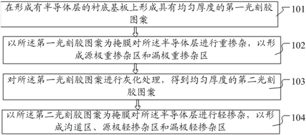
[0034] At least one embodiment of the present invention provides a method for manufacturing a thin film transistor, comprising: forming a first photoresist pattern with a uniform thickness on a base substrate formed with a semiconductor layer; using the first photoresist pattern as a mask pair The semiconductor layer is heavily doped to form a heavily doped source region and a heavily doped drain region; ashing the first photoresist pattern to obtain a second photoresist pattern with a uniform thickness; The resist pattern is used as a mask to lightly dope the semiconductor layer to form a channel region, a lightly doped source region and a lightly doped drain region.

[0035] The "half-exposure process" in the present disclosure refers to exposing the photoresist layer using, for example, a gray-tone mask or a half-tone mask. The areas of the photoresist that are exposed by the gray or half-tone areas are called half-exposed areas.

[0036] In the present invention, it is on...

Embodiment 1

[0039] This embodiment provides a method for manufacturing a thin film transistor. For example, figure 1 A process flow chart of a thin film transistor manufacturing method provided in this embodiment. include:

[0040] Step 101: forming a first photoresist pattern with a uniform thickness on the substrate on which the semiconductor layer is formed;

[0041] Step 102: using the first photoresist pattern as a mask to heavily dope the semiconductor layer to form a heavily doped source region and a heavily doped drain region;

[0042] Step 103: Perform ashing treatment on the first photoresist pattern to obtain a second photoresist pattern with a uniform thickness;

[0043] Step 104: Lightly doping the semiconductor layer by using the second photoresist pattern as a mask to form a lightly doped source region and a lightly doped drain region of the channel region.

[0044] For example, in order to more clearly illustrate the fabrication process of thin film transistors, Figu...

Embodiment 2

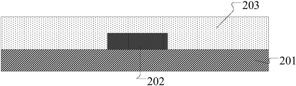
[0062] This embodiment provides a method for manufacturing a thin film transistor. Figure 3a-3h A schematic process flow diagram of another manufacturing method of a bottom-gate thin film transistor provided by an embodiment of the present invention is given.

[0063] For example, if Figure 3a As shown, a semiconductor layer thin film 204 is deposited on the first buffer layer 203, the semiconductor layer thin film 204 is doped and then coated with photoresist for patterning, so that the channel region to be formed is also doped. For example, the threshold voltage (threshold voltage, Vth) of the semiconductor layer thin film 204 is adjusted by using a doping process. For example, the doping process for adjusting the threshold voltage may be a boron ion or phosphorus ion doping implantation process for the semiconductor layer film 204 .

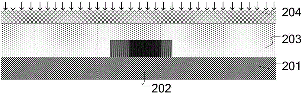
[0064] For example, if Figure 3b As shown, a photoresist (not shown) is coated on the semiconductor layer film, and the photoresist is ...


PUM


Abstract

The invention provides preparation methods of a thin film transistor and an array substrate, the array substrate and a display device. The preparation method of the thin film transistor comprises the steps of: forming a first photoresist pattern with a uniform thickness on a substrate formed with a semiconductor layer; carrying out heavy doping on the semiconductor layer employing the first photoresist pattern as a mask to form a source heavily-doped region and a drain heavily-doped region; carrying out ashing treatment on the first photoresist pattern to obtain a second photoresist pattern with the uniform thickness; and carrying out light doping on the semiconductor layer employing the second photoresist pattern as the mask to form a channel region, a source lightly-doped region and a drain lightly-doped region. By the method, a photoresist can be fully utilized; the critical sizes of the source lightly-doped region and the drain lightly-doped region are accurately and efficiently controlled; and the product uniformity is ensured.

Description

technical field [0001] Embodiments of the present invention relate to a method for preparing a thin film transistor and an array substrate, the array substrate and a display device. Background technique [0002] LTPS (Low Temperature Poly-Silicon, low-temperature polysilicon) thin film transistors (Thin Film Transistor, TFT) are widely used in display products (such as mobile phones, watches, tablet computers, etc.). LTPS technology can form a high-mobility polysilicon semiconductor layer by doping the polysilicon semiconductor layer, so that the display screen has the advantages of high resolution, high aperture ratio, high response speed and low power consumption. [0003] Since the crystal lattice of polysilicon is neatly arranged, while the electron mobility of LTPS is improved, the electrons receive less resistance inside it, which will easily lead to serious leakage current phenomenon in the off state of the thin film transistor formed by polysilicon, thus affecting po...

Claims


Application Information

Patent Timeline
Patent Type & Authority Applications(China)
IPC IPC(8): H01L21/336
CPCH01L29/66742H01L29/78645H01L27/1288H01L29/66757H01L29/78621H01L29/78633H01L2029/7863H01L21/0273H01L29/786H10K59/1213H10K71/233H10K71/00H01L27/1214H01L21/02532H01L21/02592H01L21/0262H01L21/02675H01L21/0274H01L21/26513H01L21/266H01L27/1222H01L27/1274H01L29/167H01L29/66765H01L29/78675H01L29/78678
Inventor 孙超超王超刘华锋赵生伟顺布乐杨磊胡重粮杨盟吕景萍谢霖孙士民丁多龙
Owner BOE TECH GRP CO LTD
Why Eureka
Try Eureka