Surface detect cavity photonic crystal refractive index sensor containing absorption medium graphene
A technology of refractive index sensor and photonic crystal, which is applied in the field of optical sensing, can solve the problems of poor stability and low detection accuracy of sensors, and achieve the effects of low cost, high sensitivity and strong repeatability
- Summary
- Abstract
- Description
- Claims
- Application Information
AI Technical Summary
Problems solved by technology
Method used
Image
Examples
Embodiment 1
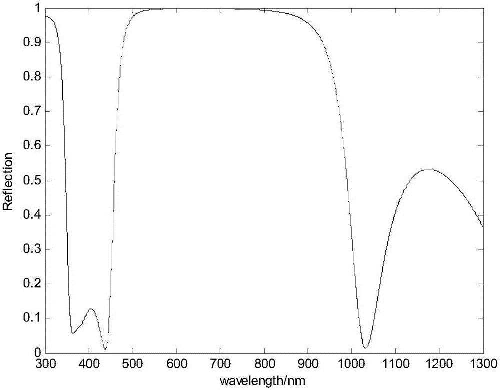
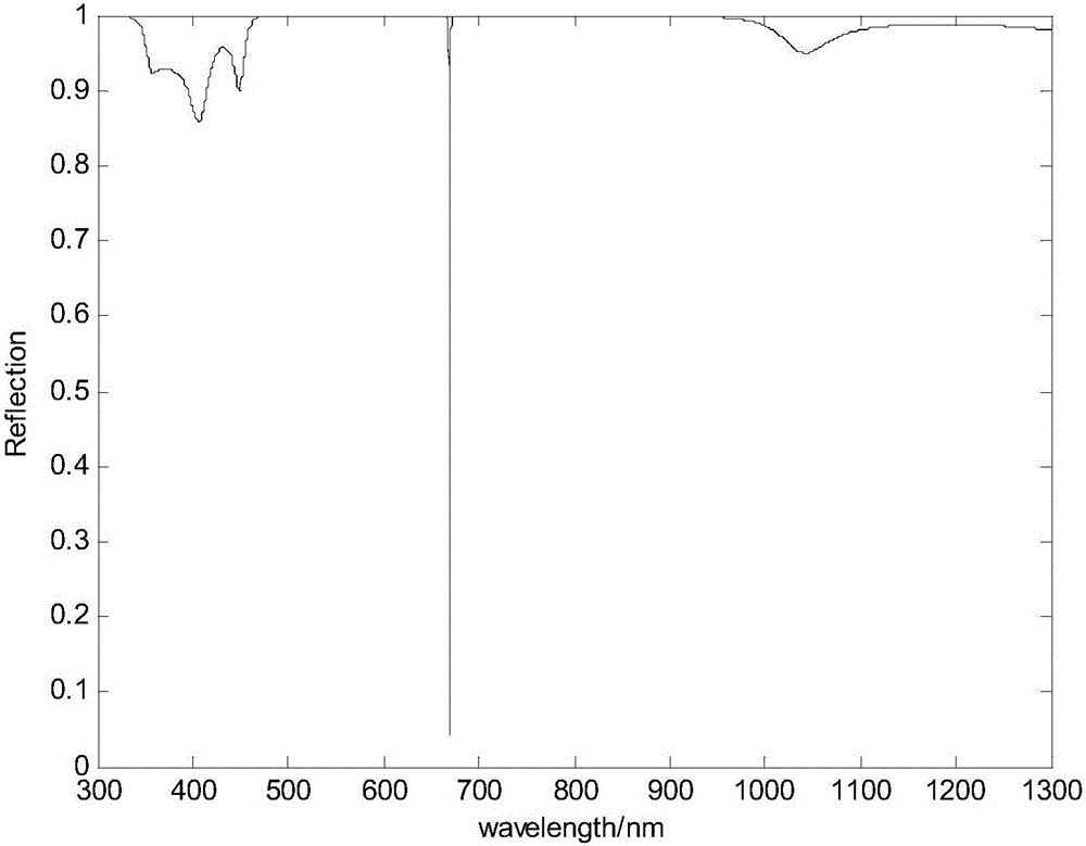
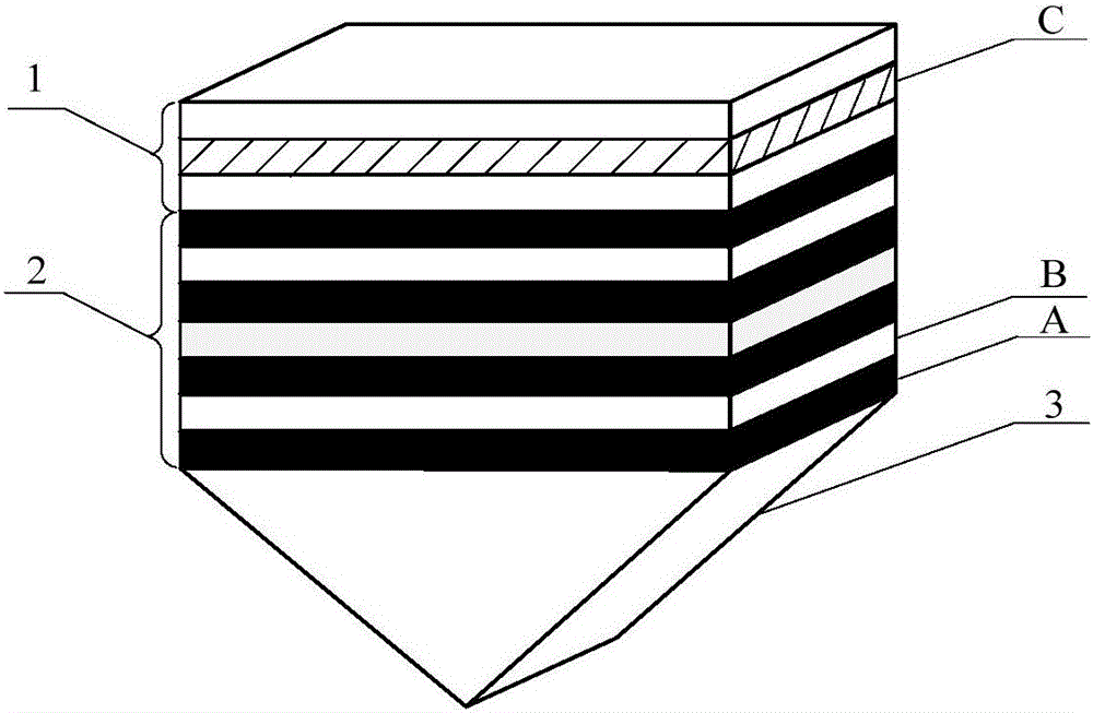
[0027] In this example, the refractive index of the high refractive index material A in the periodic photonic crystal 2 is n A =2.65 silicon carbide, low refractive index material B selects refractive index n B =1.38 magnesium fluoride, periodic photonic crystal 2 is formed by periodic arrangement of silicon carbide and magnesium fluoride, and the thickness is d respectively A =77nm and d B =147nm, the number of cycles n=3. The surface defect cavity 1 has a thickness of d 1 = 15nm and d 2 = 31nm two layers of magnesium fluoride (low refractive index material B) and the absorption medium graphene C, the absorption medium graphene C is placed between the two layers of magnesium fluoride, the number of layers is n c = 1, its structural composition is magnesium fluoride-graphene-magnesium fluoride. The NaCl solution with the concentration of c1=38% and c2=40% is selected as the sample to be tested and analyzed. The NaCl solution flows through the surface of the sensor through a micro...
Embodiment 2
[0029] In this example, the refractive index of the high refractive index material A in the periodic photonic crystal 2 is n A =2.65 titanium dioxide, low refractive index material B selects refractive index n B =1.38 silicon dioxide, periodic photonic crystal 2 is formed by periodic arrangement of titanium dioxide and silicon dioxide, and the thickness is d respectively A =77nm and d B =147nm, the number of cycles n=3. The surface defect cavity 1 has a thickness of d 1 = 13nm and d 2 = 30nm two layers of silicon dioxide (low refractive index material B) and the absorption medium graphene C are composed, and the absorption medium graphene C is placed between the two layers of silicon dioxide. Its structural composition is silica-graphene-silica, and the number of graphene layers of the absorption medium is n c = 1. The NaCl solution with the concentration of c1=40% and c2=38% is selected as the sample to be tested and analyzed. The NaCl solution flows through the surface of the ...
PUM
| Property | Measurement | Unit |
|---|---|---|
| thickness | aaaaa | aaaaa |
| thickness | aaaaa | aaaaa |
| wavelength | aaaaa | aaaaa |
Abstract
Description
Claims
Application Information


