

Preparation and fast light control method for nano pattern based on organic polymer
A nano-pattern and polymer technology, applied in photosensitive materials for opto-mechanical devices, photo-mechanical devices, and photoplate-making processes for patterned surfaces, can solve problems affecting function development and application, changing material phase structure, etc. Achieve the effects of low production cost, simple process, and easy promotion and application
- Summary
- Abstract
- Description
- Claims
- Application Information
AI Technical Summary
Problems solved by technology
Method used
Image

Examples
Embodiment 1
[0044]
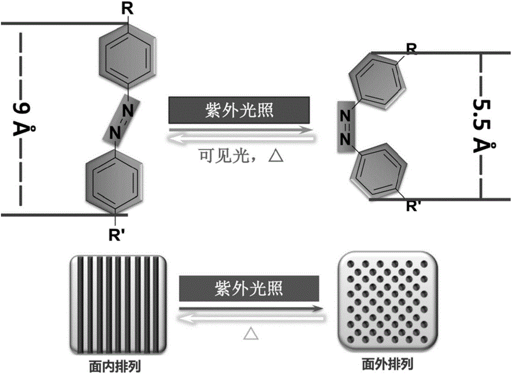
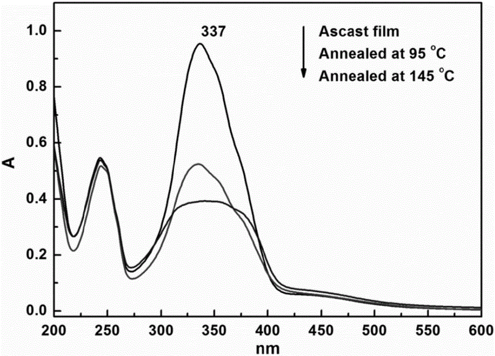
[0045] 1. Preparation of a phase-separated structure: Dissolving the polymerized block polymer 1 in an organic solvent solution such as toluene or tetrahydrofuran to obtain a homogeneous clear solution, which is fully dissolved and then filtered. Polymer thin films are formed on clean substrates by methods such as spin coating or bar coating. After the polymer film is annealed, a regular and ordered nano phase separation structure can be obtained. The structure typically has a diameter of 5-30 nanometers with a period of 10-100 nanometers. The distribution structure generally has a strip or point shape. As the main object of rapid regulation, the strip distribution is alternately arranged in parallel between different phases. The specific shape is as follows Figure 5 (a), Image 6 (a) shown.
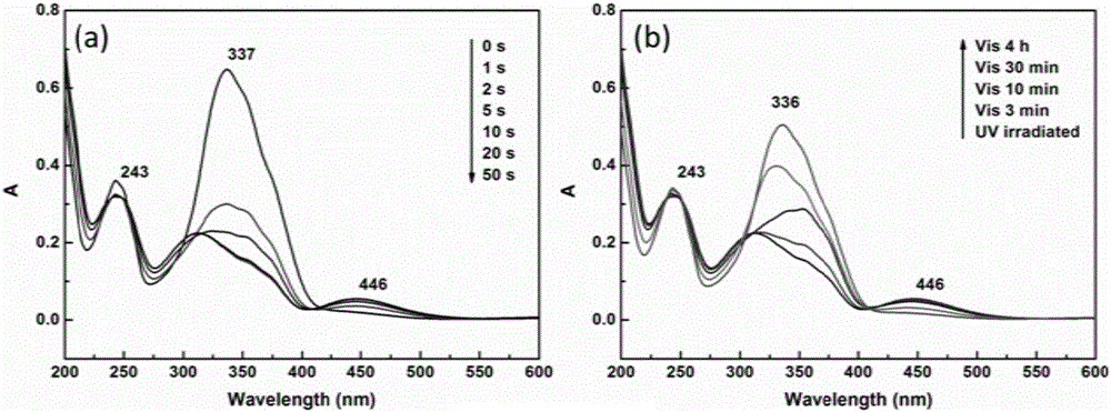
[0046] 2. Ultraviolet light response: Under certain conditions, such as room temperature, the nano-pattern of this film can change rapidly when irradiated by ultraviolet ...
Embodiment 2
[0050]
[0051] 1. Preparation of a phase-separated structure: Polymer 2 was used to prepare a polymer film, and the preparation method was the same as in Example 1.
[0052] 2. Response to ultraviolet light: the same as in Example 1.
[0053] 3. Regulation of nanopatterns by ultraviolet light: the same as in Example 1.
[0054] 4. Regulation of large-area nanopatterns: the same as in Example 1.
Embodiment 3
[0056]
[0057] 1. Preparation of a phase-separated structure: Polymer 3 was used to prepare a polymer film, and the preparation method was the same as in Example 1.
[0058] 2. Response to ultraviolet light: the same as in Example 1.
[0059] 3. Regulation of nanopatterns by ultraviolet light: the same as in Example 1.
[0060] 4. Regulation of large-area nanopatterns: the same as in Example 1.
PUM
 Abstract
Description
Claims
Application Information