Super-hydrophobic chip for enrichment and condensation of molecules as well as preparation method and application thereof
A super-hydrophobic, chip technology, applied in the analysis of materials, material excitation analysis, material analysis by optical means, etc., can solve problems such as the inability to obtain highly sensitive substrates, and achieve the effect of low solvent loss rate
- Summary
- Abstract
- Description
- Claims
- Application Information
AI Technical Summary
Problems solved by technology
Method used
Image

Examples
Embodiment 1
[0047] Step 1: Preparation of template
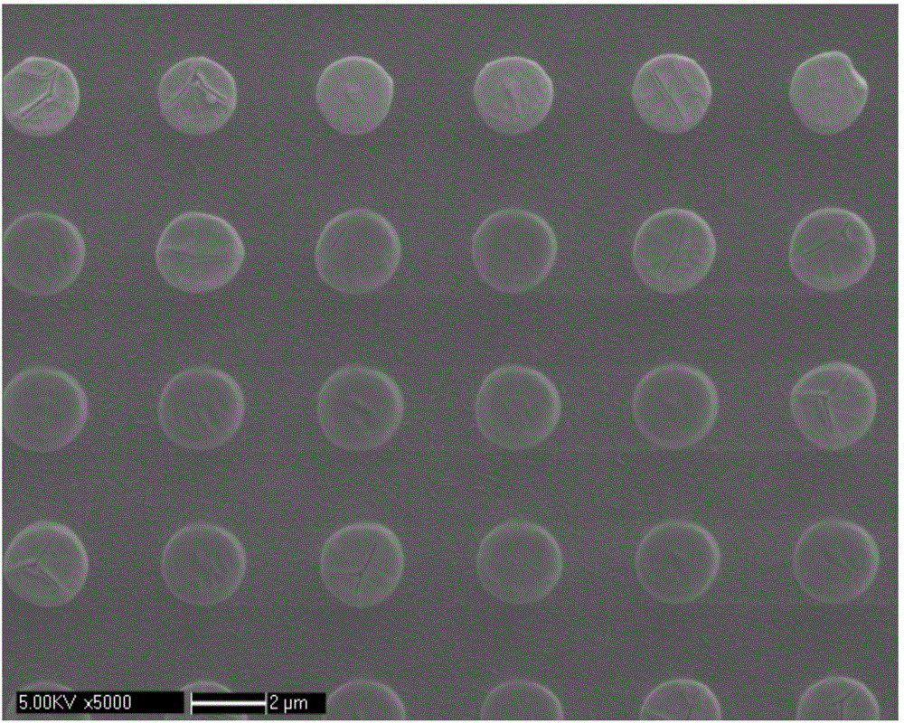
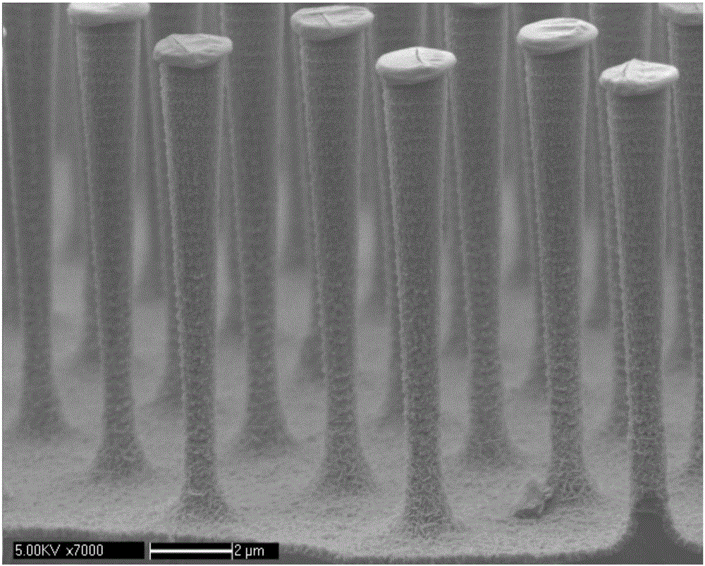
[0048] The cleaned silicon wafer is subjected to adhesion-increasing treatment, and the photoresist is evenly coated on the silicon wafer, and then baked; then the baked silicon wafer and the pattern on the photoresist board are pre-aligned and automatically aligned. Bit operation, after the bit alignment is completed, exposure treatment is performed, and then development treatment is carried out to obtain a silicon wafer with a uniform array structure pattern with a pitch of 2 microns × 2 microns ( figure 1 ), and then carry out deep silicon etching to the silicon wafer. The deep silicon etching depth is 30 microns, and the silicon wafer with a uniform silicon column array structure with an etching depth of 30 microns and a silicon column spacing of 2 microns×2 microns is obtained ( figure 2 ), and then by magnetron sputtering, the crystal film Au is sprayed on the silicon chip of the silicon column array structure to obtain the templ...
Embodiment 2
[0058] Step 1: Preparation of template
[0059] The cleaned silicon wafer is subjected to adhesion-increasing treatment, and the photoresist is evenly coated on the silicon wafer, and then baked; then the baked silicon wafer and the pattern on the photoresist board are pre-aligned and automatically aligned. Bit operation, after the bit alignment is completed, exposure treatment is carried out, and then development treatment is carried out to obtain a silicon wafer with a uniform array structure pattern with a pitch of 4 microns × 4 microns ( Figure 7 ), and then carry out deep silicon etching to the silicon wafer. The deep silicon etching depth is 30 microns, and the silicon wafer with a uniform silicon column array structure with an etching depth of 10 microns and a silicon column spacing of 4 microns×4 microns is obtained ( Figure 8 ), and then by magnetron sputtering, the crystal film Au is sprayed on the silicon chip of the silicon column array structure to obtain the te...
Embodiment 3
[0066] Step 1: Preparation of template
[0067] The cleaned silicon wafer is subjected to adhesion-increasing treatment, and the photoresist is evenly coated on the silicon wafer, and then baked; then the baked silicon wafer and the pattern on the photoresist board are pre-aligned and automatically aligned. Bit operation, after the bit alignment is completed, exposure treatment is performed, and then development treatment is carried out to obtain a silicon wafer with a uniform array structure pattern with a pitch of 2 microns × 2 microns ( Figure 12 ), and then carry out deep silicon etching to the silicon wafer. The deep silicon etching depth is 30 microns, and the silicon wafer with a uniform silicon column array structure with an etching depth of 10 microns and a silicon column spacing of 2 microns×2 microns is obtained ( Figure 13 ), and then by magnetron sputtering, the crystal film Au is sprayed on the silicon chip of the silicon column array structure to obtain the te...
PUM
| Property | Measurement | Unit |
|---|---|---|
| length | aaaaa | aaaaa |
| height | aaaaa | aaaaa |
| diameter | aaaaa | aaaaa |
Abstract
Description
Claims
Application Information
 - R&D
- Intellectual Property
- Life Sciences
- Materials
- Tech Scout
- Unparalleled Data Quality
- Higher Quality Content
- 60% Fewer Hallucinations
Browse by: Latest US Patents, China's latest patents, Technical Efficacy Thesaurus, Application Domain, Technology Topic, Popular Technical Reports.
© 2025 PatSnap. All rights reserved.Legal|Privacy policy|Modern Slavery Act Transparency Statement|Sitemap|About US| Contact US: help@patsnap.com