Composite reaction chamber extension device used for growing electronic device and growing method

A technology of electronic devices and reaction chambers, which is applied in the field of compound reaction chamber epitaxy equipment and growth, can solve the problems of poor crystal quality and high dislocation density in the growth buffer layer, so as to solve the problems of poor crystal quality, improve comprehensive performance, and improve crystal quality Effect

Inactive Publication Date: 2016-11-23
PEKING UNIV
View PDF5 Cites 3 Cited by
  • Summary
  • Abstract
  • Description
  • Claims
  • Application Information

AI Technical Summary

Problems solved by technology

[0004] In order to overcome the deficiencies of the above-mentioned prior art, the present invention provides a composite reaction chamber epitaxy equipment for growing electronic devices, including a physical deposition chamber and a chemical deposition reaction chamber, which can solve the problem of the growth buffer of metal-organic vapor deposition equipment in the prior art. Problems with poor layer crystal quality and high dislocation density

Method used


Image

  • Composite reaction chamber extension device used for growing electronic device and growing method
  • Composite reaction chamber extension device used for growing electronic device and growing method
  • Composite reaction chamber extension device used for growing electronic device and growing method

Examples


Embodiment Construction

[0029]Below in conjunction with accompanying drawing, further describe the present invention through embodiment, but do not limit the scope of the present invention in any way.

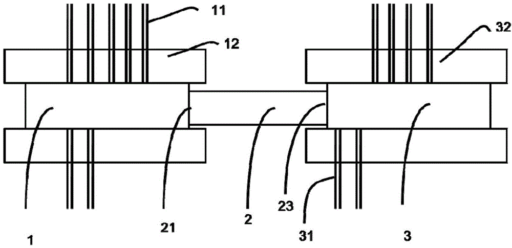
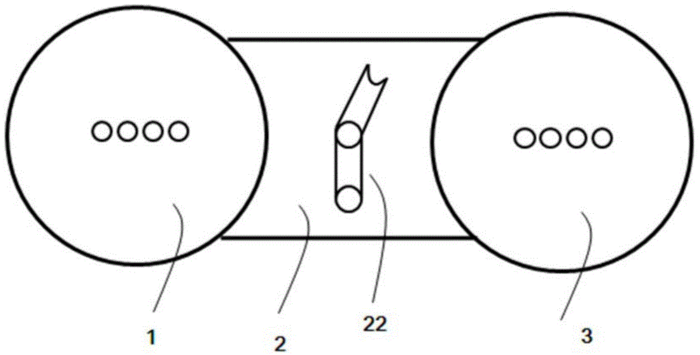
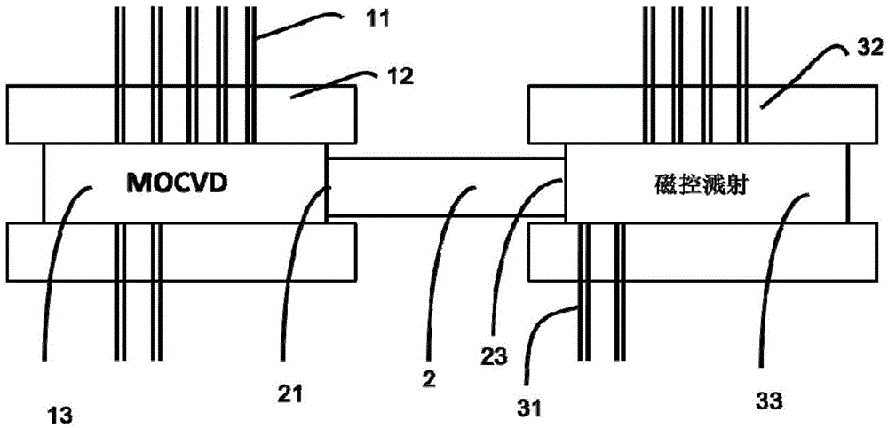
[0030] figure 1 The structural diagram of the composite reaction chamber deposition equipment provided by the present invention; figure 2 It is a top view of the composite reaction chamber deposition equipment structure of the present invention; wherein, 1 is a chemical reaction chamber; 11 is a source material delivery pipeline and a cooling water pipeline of the chemical reaction chamber; 12 is a cover plate of the chemical reaction chamber; 2 is The transfer chamber; 21 is the valve connecting the transfer chamber and the chemical reaction chamber; 22 is the manipulator of the transfer chamber; 23 is the valve connecting the transfer chamber and the physical reaction chamber; 3 is the physical reaction chamber; 31 is the source material of the physical reaction chamber Conveying pipeline and cool...


PUM


Abstract

The invention discloses a composite reaction chamber extension device used for growing an electronic device. The composite reaction chamber extension device comprises a physical deposition reaction chamber and a chemical deposition reaction chamber. Each of the two reaction chambers is provided with a source material conveying pipeline, a cooling water pipeline, a cover plate, a controller and a sample tray, and the two reaction chambers are connected with each other through a transfer chamber and used for conveying samples. According to the composite reaction chamber extension device, the beneficial effects of physical deposition and chemical deposition are fully utilized, and a buffering layer and a transition layer needed for heteroepitaxy are deposited through the physical deposition reaction chamber and are transmitted to the chemical deposition reaction chamber through the transfer chamber to deposit a device structure. According to the composite reaction chamber extension device, deposition from the physical deposition reaction chamber to the chemical deposition reaction chamber can be achieved, and the purpose that chemical deposition is achieved firstly, and then physical deposition is conducted can be achieved. The problems that due to the fact that a metal organic vapor deposition device is utilized for growing a buffering layer in the prior art, the quality of crystals is poor, and the dislocation density is high can be solved, and industrialization and functionization of the device are facilitated.

Description

technical field [0001] The invention belongs to the technical field of semiconductor material growth equipment, and relates to epitaxial growth equipment for growing electronic devices on a substrate, in particular to a compound reaction chamber epitaxial equipment and a growth method for growing electronic devices. Background technique [0002] In recent years, the third-generation wide-bandgap semiconductor material gallium nitride and its III / V series nitrides have made remarkable achievements in the fields of lighting and electronics industries. Due to the excellent physical and chemical properties of gallium nitride materials, it has been widely used. For example, gallium nitride-based light-emitting diodes on sapphire substrates have been widely used in the field of lighting. Existing research also shows that gallium nitride has potential applications in solar cells, ultraviolet detectors, lasers, electronic devices and other fields. [0003] At present, the material...

Claims


Application Information

Patent Timeline
Patent Type & Authority Applications(China)
IPC IPC(8): C23C16/44C23C14/22C30B25/02C30B23/02
Inventor 罗睿宏吴洁君张国义
Owner PEKING UNIV
Why Eureka
Try Eureka