A kind of preparation method of smart window
A technology of smart windows and substrates, applied in the field of OLED display, can solve the problems of low power consumption, complex structure, disadvantages, etc., and achieve the effects of reducing total reflection loss, large application potential, and simple structure
- Summary
- Abstract
- Description
- Claims
- Application Information
AI Technical Summary
Problems solved by technology
Method used
Image
Examples
Embodiment 1
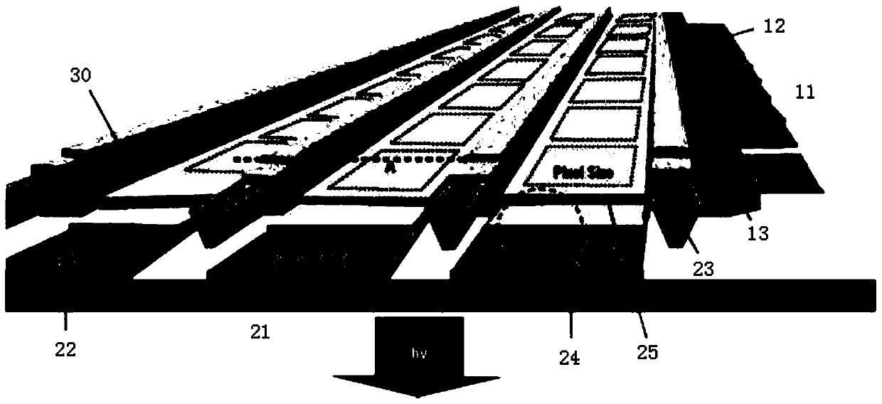
[0033] Smart windows include two categories based on different OLED structures: Passive Matrix Organic Light Emitting Diode (PMOLED for short) and Active Matrix Organic Light Emitting Diode (AMOLED for short). ).
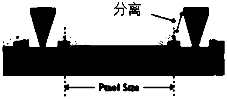
[0034] Picture 1-1 Shows the structure of a passive matrix organic light emitting diode PMOLED, including an anode part 11, an anode transparent conductive film ITO 12, an insulating layer (PR or PI) 13, a cathode part 21, a cathode transparent conductive film ITO 22, a cathode separator or a side wall 23 and cathode contactor 24, cathode metal strip (film) 25, a plurality of organic layers 30; Figure 1-2 for Picture 1-1 Schematic diagram of the cross-section in A.
[0035] The preparation method of the smart window involved in this embodiment is described as follows:
[0036] (1) Combining passive matrix organic light-emitting diode PMOLED and polymer dispersed liquid crystal (Polymer Dispersed Liquid Crystal, referred to as: PDLC) preparation, including the f...
Embodiment 2
[0055] Figure 5 It is a schematic diagram of the pixel structure of AMOLED; the pixel structure of AMOLED includes anode, cathode, organic layer, and TFT array.
[0056] The preparation method of the smart window involved in this embodiment is described as follows:
[0057] (1) Combining active matrix organic light-emitting diode AMOLED with polymer dispersed liquid crystal (Polymer Dispersed Liquid Crystal, referred to as: PDLC) preparation, including the following steps:
[0058] 1) Thin film transistor array preparation step: prepare a thin film transistor TFT array on the substrate, the TFT array includes one or more of amorphous silicon TFT, polysilicon TFT, oxide TFT, and organic TFT, preferably oxide TFT and organic TFT.
[0059] The TFT structure may be one or more of bottom gate bottom contact, bottom gate top contact, top gate bottom contact, top gate top contact, and double gate. If it is a bottom-gate TFT, either a BCE (Back Channel Etch, reverse channel etching...
PUM
 Abstract
Description
Claims
Application Information


