Chip packaging structure for slowing down electromagnetic interference and packaging method

A chip packaging structure, electromagnetic interference technology, applied in the direction of circuits, electrical components, electric solid devices, etc., can solve the problems of affecting signal transmission quality, line impedance mismatch, line noise increase, etc., to reduce the signal between lines inside the chip crosstalk, improved packaging reliability, and simple process

Active Publication Date: 2016-11-30
HUATIAN TECH KUNSHAN ELECTRONICS
View PDF5 Cites 8 Cited by
  • Summary
  • Abstract
  • Description
  • Claims
  • Application Information

AI Technical Summary

Problems solved by technology

Following the development trend of miniaturization, high density and multi-function of electronic packaging, the number of components on the circuit board increases, the distance between adjacent components is shortened, the probability of radiation interference between components during circuit operation is greatly increased, and the line impedance mismatch and line noise Phenomena increase and affect the quality of signal transmission

Method used


Image

  • Chip packaging structure for slowing down electromagnetic interference and packaging method
  • Chip packaging structure for slowing down electromagnetic interference and packaging method
  • Chip packaging structure for slowing down electromagnetic interference and packaging method

Examples


Embodiment 1

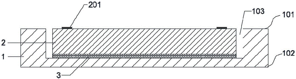
[0055] like Figure 11 and Figure 12 As shown, a chip packaging structure for mitigating electromagnetic interference includes a silicon substrate 1 and a chip 2, the silicon substrate has a first surface 101 and a second surface 102 opposite to it, and at least A sinking groove 103 facing the second surface, the sinking groove is preferably a straight groove or an inclined groove with an angle between the side wall and the bottom surface of 80-120, which is not limited here. The schematic diagram of this embodiment is in the shape of a straight groove. At least one chip 2 can be placed in the sinking groove. In this embodiment, a chip is placed, and the front of the chip is close to the first surface; specifically, the back of the chip is pasted with an adhesive 3 Installed to the groove bottom of the sinking groove to realize chip mounting, to better fix the chip and prevent the chip from shifting. The front side of the chip includes a pad 201; a first insulating layer 4...

Embodiment 2

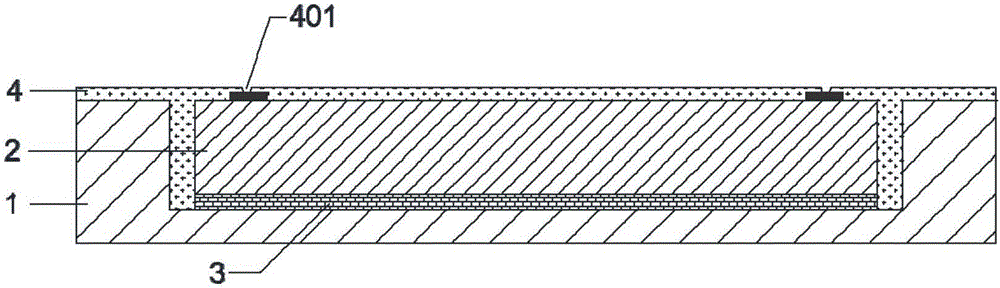
[0089] like Figure 13 and Figure 14 As shown, a chip packaging structure for mitigating electromagnetic interference includes a silicon substrate 1 and a chip 2. The silicon substrate has a first surface 101 and a second surface 102 opposite to it. The sunken groove 103 on the surface, at least one chip is mounted on the bottom of the sunken groove with the back facing down, and the front of the chip contains a solder pad 201; between the peripheral side of the chip and the side wall of the sunken groove, the front of the chip And the first insulating layer 4 is formed on the first surface; the first metal rewiring 501, the first inductance wiring 502 that goes around continuously, and at least two first capacitance wirings with a dielectric layer in between are formed on the first insulating layer. 503, the first metal rewiring, the first inductance wiring, and the first capacitor wiring are electrically connected to the pads of the chip through the first insulating layer;...


PUM


Abstract

The invention discloses a chip packaging structure for slowing down electromagnetic interference and a packaging method thereof. The packaging method comprises the following steps: producing a sinking groove in a silicon substrate, and embedding a chip whose front surface is upwards arranged and provided with welding pads into the sinking groove to save the packaging space; and forming horizontally-arranged or vertically-arranged inductance distribution wires on the front surface of the chip and a first surface of the silicon substrate, forming horizontally-arranged or vertically-arranged capacitance distribution wires on a first insulation layer, and extending a first metal redistribution wire or a second metal redistribution wire and solder balls to the surface of the silicon substrate to ensure that the welding pads of the chip are electrically fanned out of the surface of the silicon substrate and purposes of improving the packaging reliability and achieving simple process and low cost can be achieved. The horizontally-arranged or vertically-arranged inductance distribution wires form an inductor, and the horizontally-arranged or vertically-arranged capacitance distribution wires and dielectric layers among the capacitance distribution wires form a capacitor; and by adopting the inductor and capacitor with filter characteristics, the signal crosstalk among circuits in the chip can be reduced, unnecessary electric signals can be removed by filtration, the reliability and performance of packaged products can be enhanced, and the cost can also be reduced.

Description

technical field [0001] The invention relates to the field of semiconductor packaging, in particular to a chip packaging structure and packaging method for alleviating electromagnetic interference. technical background [0002] After completing the first-level packaging, the chip needs to be surface-mounted on a printed circuit board to connect to other components to realize its functions. Following the development trend of miniaturization, high density and multi-function of electronic packaging, the number of components on the circuit board increases, the distance between adjacent components is shortened, the probability of radiation interference between components during circuit operation is greatly increased, and the line impedance mismatch and line noise Phenomena increase and affect the quality of signal transmission. [0003] In general, circuit boards use embedded capacitors and inductors to reduce the impact of the above phenomena. While reducing the packaging area ...

Claims


Application Information

Patent Timeline
Patent Type & Authority Applications(China)
IPC IPC(8): H01L21/56H01L23/00H01L23/31H01L23/522
CPCH01L2224/04105H01L2224/12105H01L2224/19H01L2224/32225H01L2224/73267H01L2224/92244H01L2924/15153H01L23/3121H01L21/56H01L23/522H01L23/5223H01L23/5227H01L24/85
Inventor 于大全项敏
Owner HUATIAN TECH KUNSHAN ELECTRONICS
Why Eureka
Try Eureka