Silicon-based ultraviolet photoelectric detector based on graphene and fabrication method of silicon-based ultraviolet photoelectric detector

A technology of electrical detectors and ultraviolet light, which is applied in the field of sensing, can solve the problems of blocking ultraviolet light and low optical response of photoelectric sensors, and achieve the effects of increasing ultraviolet response, reducing recombination, and improving response speed

Inactive Publication Date: 2016-11-30
杭州紫元科技有限公司
View PDF4 Cites 27 Cited by
  • Summary
  • Abstract
  • Description
  • Claims
  • Application Information

AI Technical Summary

Problems solved by technology

However, the metal has a strong reflection and absorption effect on the incident ultraviolet light, which prevents the ultraviolet

Method used


Image

  • Silicon-based ultraviolet photoelectric detector based on graphene and fabrication method of silicon-based ultraviolet photoelectric detector
  • Silicon-based ultraviolet photoelectric detector based on graphene and fabrication method of silicon-based ultraviolet photoelectric detector
  • Silicon-based ultraviolet photoelectric detector based on graphene and fabrication method of silicon-based ultraviolet photoelectric detector

Examples


Embodiment 1

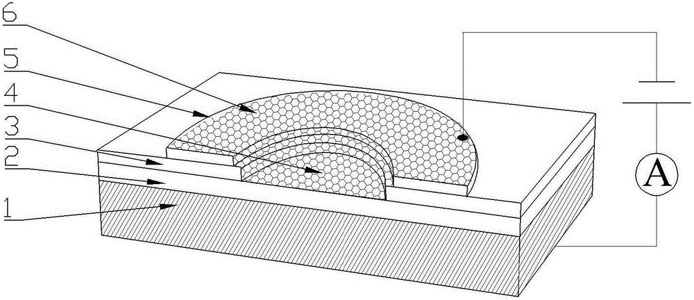
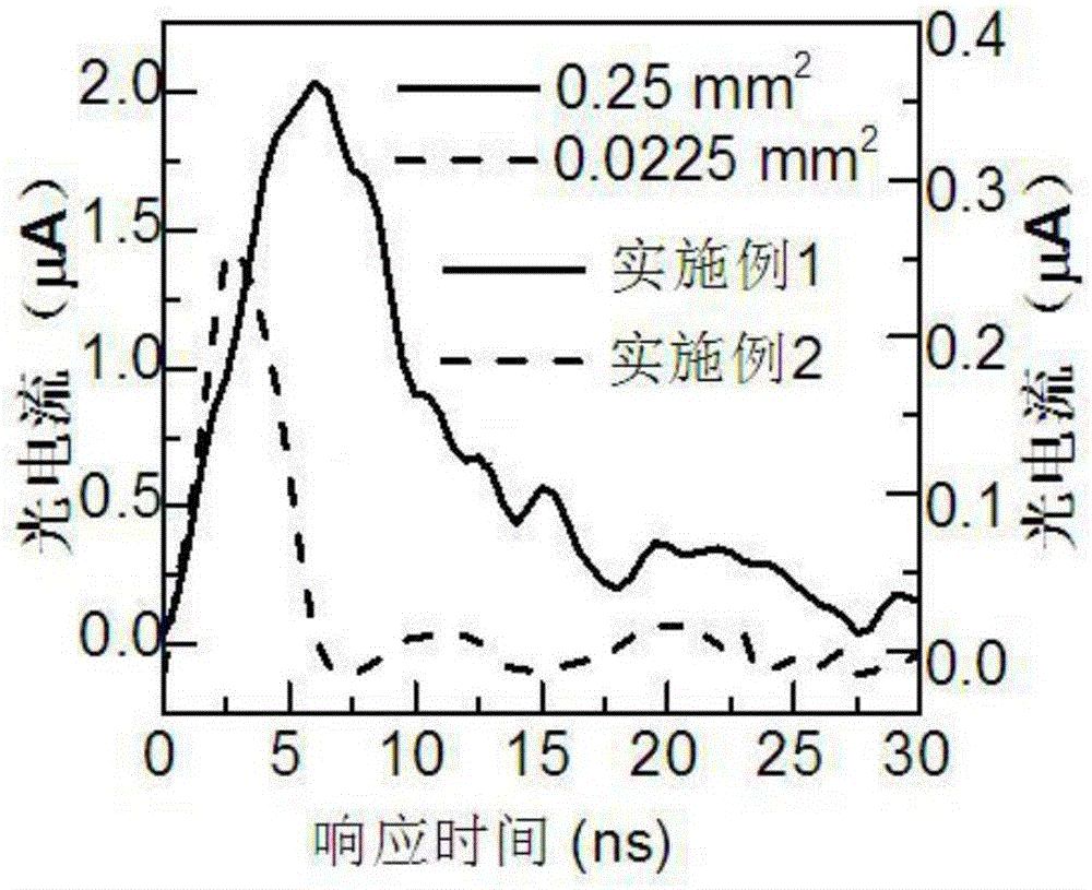
[0035] Depend on figure 1 As shown, a graphene-based silicon-based ultraviolet photodetector of this embodiment includes an epitaxial silicon wafer substrate, and the epitaxial silicon wafer substrate includes an N-type doped heavily doped layer 1 located in the lower layer and an upper layer N-type doped lightly doped layer 2, the doping concentration of heavily doped layer 1 is greater than 4.5×10 18 cm -3 , the thickness of the heavily doped layer 1 is 180-500 μm, and the doping concentration of the lightly doped layer 2 is 1×10 16 ~1×10 14 cm -3 , the thickness of the lightly doped layer 2 is 10-2000nm; the upper surface of the lightly doped layer 2 is provided with a silicon dioxide isolation layer 3 with a thickness of 300nm, and the center of the silicon dioxide isolation layer 3 is provided with a circular silicon dioxide layer with a photosensitive area. Window 4, photosensitive area is 0.25mm 2 The upper surface of the silicon dioxide isolation layer 3 is also p...

Embodiment 2

[0043] Depend on figure 1 As shown, a graphene-based silicon-based ultraviolet photodetector of this embodiment includes an epitaxial silicon wafer substrate, and the epitaxial silicon wafer substrate includes a P-type doped heavily doped layer 1 located in the lower layer and an upper layer P-type doped lightly doped layer 2, the doping concentration of heavily doped layer 1 is greater than 8×10 18 cm -3 , the thickness of the heavily doped layer 1 is 250-400 μm, and the doping concentration of the lightly doped layer 2 is 3×10 14 ~5×10 15 cm -3 , the thickness of the lightly doped layer 2 is 20-500nm; the upper surface of the lightly doped layer 2 is provided with a silicon dioxide isolation layer 3 with a thickness of 300nm, and the center of the silicon dioxide isolation layer 3 is provided with a circular silicon Window 4, photosensitive area is 0.0225mm 2 The upper surface of the silicon dioxide isolation layer 3 is also provided with a chromium / gold metal film top ...

Embodiment 3

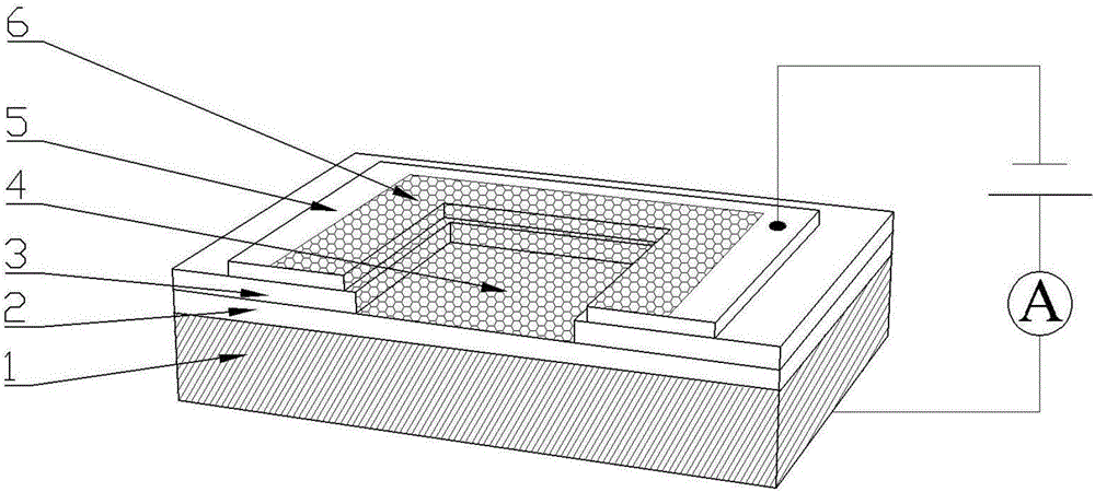
[0052] Such as image 3 As shown, a graphene-based silicon-based ultraviolet photodetector (array type) of the present embodiment includes an epitaxial silicon wafer substrate, and the epitaxial silicon wafer substrate includes an N-type doped heavily doped layer 1 located at the lower layer and the N-type doped lightly doped layer 2 located on the upper layer, and the doping concentration of the heavily doped layer 1 is greater than 8×10 18 cm -3 , the thickness of the heavily doped layer 1 is 250-400 μm, and the doping concentration of the lightly doped layer 2 is 3×10 14 ~5×10 15 cm -3 , the thickness of the lightly doped layer 2 is 20-500nm; the upper surface of the lightly doped layer 2 is provided with a silicon dioxide isolation layer 3 with a thickness of 300nm, and a rectangular silicon window with a photosensitive area is opened in the center of the silicon dioxide isolation layer 3 4. The upper surface of the silicon dioxide isolation layer 3 is also provided wi...


PUM

PropertyMeasurementUnit
Thicknessaaaaaaaaaa
Doping concentrationaaaaaaaaaa
Thicknessaaaaaaaaaa

Abstract

The invention discloses a silicon-based ultraviolet photoelectric detector based on graphene. The silicon-based ultraviolet photoelectric detector comprises an epitaxial silicon substrate, an isolation layer, a silicon window, a top electrode and a graphene thin film which are sequentially laminated, and the epitaxial silicon substrate is provided with a heavily-doped layer and a light-doped layer. The fabrication method comprises the following steps of sequentially planting the isolation layer and the top electrode on the epitaxial silicon substrate after the epitaxial silicon substrate is fabricated, etching the silicon window, and moving the graphene thin film in the silicon window and the top electrode for complete fabrication. An ultra-shallow junction design formed by a graphene/silicon structure is used for improving ultraviolet wave band response; the surface recombination is reduced by epitaxial growth of a thin silicon light-doped structure on an upper surface of the heavily-doped bottom layer, the ultraviolet response is effectively improved, the visible light response is suppressed, and the spectral selectivity detection is achieved; and with the adoption of the high-conductivity graphene thin film, extra ultraviolet light is absorbed, and the ultraviolet sensitivity and the response speed can be improved and are approximate to or even exceed a theoretical performance limit of a traditional silicon-based ultraviolet detector.

Description

technical field [0001] The invention belongs to the field of sensing technology, and relates to a photoelectric sensing device, in particular to a silicon-based ultraviolet-enhanced photodetector with a Schottky ultra-shallow junction based on a graphene film and a preparation method thereof. Background technique [0002] Ultraviolet photoelectric detection technology has a wide range of applications in ultraviolet radiation detection, environmental monitoring, chemical composition analysis, sewage detection and treatment, disaster warning, food hygiene, medical health, wireless encrypted communication, etc. Because wide bandgap semiconductors (WBG, such as gallium nitride, silicon carbide, zinc oxide, etc.) have the property of not absorbing visible light, they have received extensive attention in the field of ultraviolet detection, and a large number of researches and applications have been carried out. However, the current process for preparing large-area high-quality sin...

Claims


Application Information

Patent Timeline
IPC IPC(8): H01L31/108H01L31/028H01L31/18
CPCH01L31/028H01L31/108H01L31/1804Y02P70/50
Inventor 万霞
Owner 杭州紫元科技有限公司
Why Eureka
Try Eureka