Epitaxial structure of semiconductor ultraviolet detector chip, preparation method of epitaxial structure and semiconductor ultraviolet detector chip

A technology of ultraviolet detector and epitaxial structure, which is applied in the field of ultraviolet detector, can solve the problems of large dark current and low spectral responsivity, and achieve the effect of reducing dark current, reducing dislocation density and improving ultraviolet responsivity

Active Publication Date: 2022-01-21
ZHIXIN SEMICON (HANGZHOU) CO LTD
View PDF8 Cites 1 Cited by
  • Summary
  • Abstract
  • Description
  • Claims
  • Application Information

AI Technical Summary

Problems solved by technology

However, due to the poor quality of AlGaN materials, AlGaN ultraviolet solar blind detectors have problems such as large dark current and low spectral responsivity.

Method used


Image

  • Epitaxial structure of semiconductor ultraviolet detector chip, preparation method of epitaxial structure and semiconductor ultraviolet detector chip
  • Epitaxial structure of semiconductor ultraviolet detector chip, preparation method of epitaxial structure and semiconductor ultraviolet detector chip
  • Epitaxial structure of semiconductor ultraviolet detector chip, preparation method of epitaxial structure and semiconductor ultraviolet detector chip

Examples


preparation example Construction

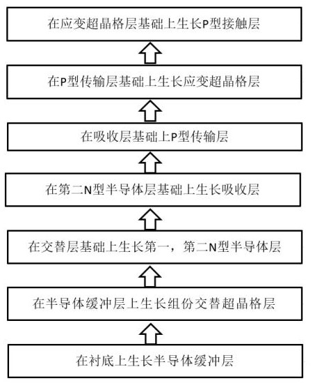
[0081] according to figure 1 The process shown in the present invention also provides a method for preparing the epitaxial structure described in the above technical solution, including the following steps:

[0082] growing a semiconductor buffer layer, alternately grown superlattice layers, a first N-type semiconductor layer, a second N-type semiconductor layer, an ultraviolet light absorbing layer, a strained superlattice layer and a P-type contact layer in sequence on the upper surface of the substrate, The epitaxial structure is obtained.

[0083] Before the epitaxial structure is grown on the upper surface of the substrate, the substrate is preferably pretreated, and the pretreatment includes sequential baking and cleaning; in the present invention, the baking is preferably performed after the The substrate is placed in a reactor and baked at 1100°C in a hydrogen atmosphere. The present invention does not have any special restrictions on the cleaning process. It is carri...

Embodiment 1

[0103] Put the sapphire substrate into the MOCVD equipment, pass through hydrogen, and after baking at 1100°C, clean the oxides and impurities on the surface of the sapphire substrate;

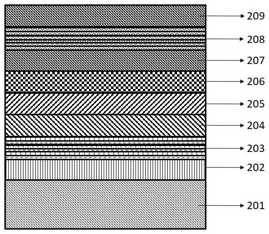
[0104] AlN layers (thickness 1.5 μm) were grown sequentially on the surface of the cleaned sapphire substrate, and AlN layers (thickness 1 nm) and Al 0.85 Ga 0.15 N layer (thickness 2nm) 50 cycles, grow N-type doped Al 0.65 Ga 0.35 N layer (thickness 1μm, N-type doping concentration 5×10 18 cm -3 ), growing N-type doped Al 0.5 Ga 0.5 N layer (thickness 1 μm, doping concentration 1×10 19 cm -3 ), growing non-doped Al 0.4 Ga 0.6 N layer (thickness 150nm), growth of P-type doped Al 0.4 Ga 0.6 N transport layer (thickness 100nm, P-type doping concentration 1×10 19 cm -3 ), growing P-type doped Al 0.4 Ga 0.6 N contact layer (thickness 10nm, doping concentration 1×10 19 cm -3 ), growing P-type doped Al 0.01 Ga 0.99 N contact layer (thickness 100nm, doping concentration 2×10 19 cm...

Embodiment 2

[0112] Put the sapphire substrate into the MOCVD equipment, pass through hydrogen, and after baking at 1100°C, clean the oxides and impurities on the surface of the sapphire substrate;

[0113] AlN layers (thickness 1.5 μm) were grown sequentially on the surface of the cleaned sapphire substrate, and AlN layers (thickness 1 nm) and Al 0.85 Ga 0.15 N layer (thickness 2nm) 50 cycles, grow N-type doped Al 0.75 Ga 0.25 N layer (thickness 1μm, N-type doping concentration 5×10 18 cm -3 ), growing N-type doped Al 0.55 Ga 0.45 N layer (thickness 1 μm, doping concentration 1×10 19 cm -3 ), growing non-doped Al 0.4 Ga 0.6 N layer (thickness 150nm), growth of P-type doped Al 0.4 Ga 0.6 N transport layer (thickness 1.5nm, P-type doping concentration 1×1019 cm -3 ), growing P-type doped Al 0.25 Ga 0.75 N contact layer (thickness 1.0nm, doping concentration 1×10 19 cm -3 ), repeatedly growing the above-mentioned P-type doped Al 0.4 Ga 0.6 N transport layer and P type doped...


PUM

PropertyMeasurementUnit
thicknessaaaaaaaaaa
thicknessaaaaaaaaaa
thicknessaaaaaaaaaa

Abstract

The invention relates to the technical field of ultraviolet detectors, in particular to an epitaxial structure of a semiconductor ultraviolet detector chip, a preparation method of the epitaxial structure and the semiconductor ultraviolet detector chip. According to the invention, through the arrangement of alternately grown superlattice layers, the dislocation line of a semiconductor buffer layer is effectively blocked, so that the dislocation density of the whole buffer layer is greatly reduced, and the problem that the dark current of a device is large due to the fact that the dislocation density is too large is solved; a strained superlattice layer is introduced between a P-type transmission layer and a P-type contact layer, and the introduction of the strained superlattice layer enables the structure to generate strain, enables an energy band to be bent, obviously improves the electron hole tunneling migration effect, improves the quantum efficiency, and improves the ultraviolet responsivity; and the introduction of the strain superlattice layer can effectively prevent the extension of dislocation lines of the bottom layer material, so that the dark current of the device can be greatly reduced, and the performance of the ultraviolet solar blind detector is improved.

Description

technical field [0001] The invention relates to the technical field of ultraviolet detectors, in particular to an epitaxial structure of a semiconductor ultraviolet detector chip, a preparation method thereof, and a semiconductor ultraviolet detector chip. Background technique [0002] Semiconductor detection devices are widely used in many fields due to their excellent characteristics, especially ultraviolet semiconductor detectors have attracted much attention due to their military and civilian applications. Because the atmosphere has the effect of scattering and absorbing ultraviolet rays, the amount of ultraviolet rays on the surface of the earth is relatively small, and the wavelengths less than 280nm are almost completely absorbed by the atmosphere, which is called the sun-blind band. The solar-blind ultraviolet detector can track and detect the tail flame of the missile, and this detection is not interfered by the ultraviolet rays generated by the sun. It has strong a...

Claims


Application Information

Patent Timeline
Patent Type & Authority Applications(China)
IPC IPC(8): H01L31/0352H01L31/105H01L31/18B82Y30/00B82Y40/00
CPCH01L31/105H01L31/1852H01L31/1848H01L31/03529B82Y30/00B82Y40/00Y02E10/544Y02P70/50
Inventor 黄小辉倪逸舟
Owner ZHIXIN SEMICON (HANGZHOU) CO LTD
Why Eureka
Try Eureka