Roughened epitaxial wafer-based electrode color difference improvement method of LED chip

A technology of LED chips and epitaxial wafers, applied in circuits, electrical components, semiconductor devices, etc., can solve problems such as chromatic aberration, pollution, wafer pollution, etc., and achieve the effect of eliminating abnormal chromatic aberration, high probability of light reflection, and improved photoelectricity

Inactive Publication Date: 2016-12-07
QUANZHOU SANXING FIRE FIGHTING EQUIP
View PDF11 Cites 1 Cited by
  • Summary
  • Abstract
  • Description
  • Claims
  • Application Information

AI Technical Summary

Problems solved by technology

[0008] 2. Epitaxy influence, that is, when preparing the GaN epitaxial layer, the density (hardness) of the N-type layer and the P-type layer has a large difference, and the surface roughness will also have a large difference after ICP dry etching
[0009] 3. Pollution effect. The wafer is polluted before ICP dry etching, which will cause the surface of the N-type layer to be etched uncleanly after ICP dry etching, and chromatic aberration will also occur.
Although this solution effectively solves the problem of electrode color difference, the N electrode only uses a part of the area to conduct current, which will definitely affect the electrical properties of the chip, resulting in high voltage
If the area of ​​the N electrode is increased to reduce the voltage, the production cost will increase (the main material of the electrode is metal gold), and the effect will not be satisfactory.
This way of sacrificing electrical properties to improve chromatic aberration is just a way of tearing down the east wall to make up for the west wall, not an ideal solution

Method used


Image

  • Roughened epitaxial wafer-based electrode color difference improvement method of LED chip
  • Roughened epitaxial wafer-based electrode color difference improvement method of LED chip
  • Roughened epitaxial wafer-based electrode color difference improvement method of LED chip

Examples


Embodiment Construction

[0049] To further illustrate the various embodiments, the present invention is provided with accompanying drawings. These drawings are a part of the disclosure of the present invention, which are mainly used to illustrate the embodiments, and can be combined with related descriptions in the specification to explain the operating principles of the embodiments. With reference to these contents, those skilled in the art should understand other possible implementations and advantages of the present invention. Components in the figures are not drawn to scale, and similar component symbols are generally used to denote similar components.

[0050] The present invention will be further described in conjunction with the accompanying drawings and specific embodiments.

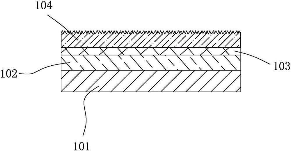
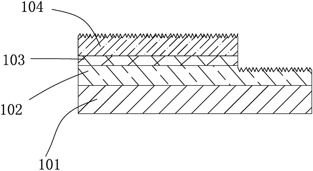
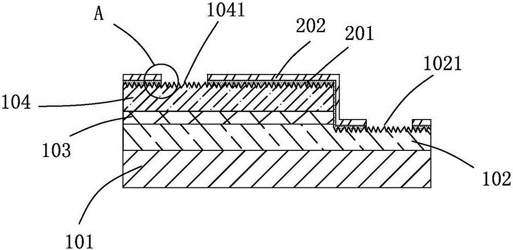
[0051] A method for improving electrode chromatic aberration of an LED chip based on roughened epitaxial wafers provided by the present invention comprises the following steps:

[0052] S1, providing a roughened GaN epit...


PUM


Abstract

The invention provides a roughened epitaxial wafer-based electrode color difference improvement method of an LED chip. The surfaces of a GaN epitaxial wafer in abdicating regions for subsequently preparing electrodes are etched to flat, so that the surface roughness is the same; the electrodes are free of a color difference after being prepared; color difference exception is completely eliminated; the cost caused by the color difference exception is reduced; a transparent conductive layer and the electrodes are subsequently prepared; and the regions are in smooth connection, the current resistance is small, diffusion is fast, the light reflection probability is high and the photoelectricity of the LED chip is also improved to a certain extent.

Description

technical field [0001] The invention relates to the field of LED chips, in particular to a method for improving electrode color difference of LED chips based on roughened epitaxial wafers. Background technique [0002] LED (Light Emitting Diode), light-emitting diode, is a solid-state semiconductor device that can convert electrical energy into visible light, and it can directly convert electricity into light. Compared with ordinary lamps (incandescent lamps, etc.), the emergence of LED lamps has the advantages of energy saving, long life, good applicability, short response time, and environmental protection. [0003] In the manufacturing process of blue and green LED chips, the mainstream method of preparing epitaxial wafers of LED chips is to sequentially deposit N-type layer, light-emitting layer and P-type layer formed by GaN doped with different ions on the sapphire substrate. GaN epitaxial wafers are divided into flat wafers and rough wafers. Flat wafers and coarse wa...

Claims


Application Information

Patent Timeline
Patent Type & Authority Applications(China)
IPC IPC(8): H01L33/00H01L33/22
CPCH01L33/22H01L33/0054
Inventor 肖君岩
Owner QUANZHOU SANXING FIRE FIGHTING EQUIP
Why Eureka
Try Eureka