OLED device

A technology of devices and electron transport layers, which is applied in the field of OLED devices, can solve problems such as device efficiency decline, poor contact surface adhesion, and lifespan decline, and achieve the effects of reducing luminescence quenching, slowing down material deterioration, and slowing down decline

Inactive Publication Date: 2016-12-07
EVERDISPLAY OPTRONICS (SHANGHAI) CO LTD
View PDF12 Cites 5 Cited by
  • Summary
  • Abstract
  • Description
  • Claims
  • Application Information

AI Technical Summary

Problems solved by technology

[0005] The essential deterioration factors are very complicated, and can be roughly divided into the following categories at present: 1) The stability of the organic film, the low glass transition temperature will make the stability of the organic film worse, which will easily lead to poor stability of the device. Therefore, improving the glass of the material The stability of the film will also be improved if the transition temperature is lowered, and it is not easy to form a crystalline film; 2) the contact surface between the anode and the organic layer is prone to the problem of poor adhesion of the contact surface due to the different types of materials, and the anode and the organic layer The greater the energy level difference of the hole injection or transport layer, the more obvious the brightness attenuation of the device and the shorter the lifetime; 3) the stability of the excited state, the more stable the excited state, the longer the lifetime of the device; 4) The electrochemical reversibility of organic materials Because the conduction process of carriers in organic thin films is a series of redox reactions, organic materials have reversible electrochemical redox properties, which can improve the stability of materials and avoid the degradation of device brightness caused by the degradation of organic materials; 5) Movable ionic impurities, mobile ions caused by diffusion from the electrode (such as IN 3+ , Sn 4+ ) is very likely to become an electron and hole recombination center or a quenching center, so that the efficiency of the device will decline and the lifetime will decrease; and there is no functional layer structure for improving the OLED lifetime.

Method used


Image

  • OLED device
  • OLED device
  • OLED device

Examples


Embodiment Construction

[0029] The present invention will be further described below in conjunction with the accompanying drawings and specific embodiments, but not as a limitation of the present invention.
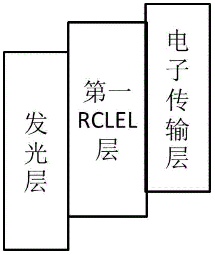
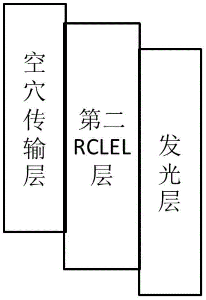
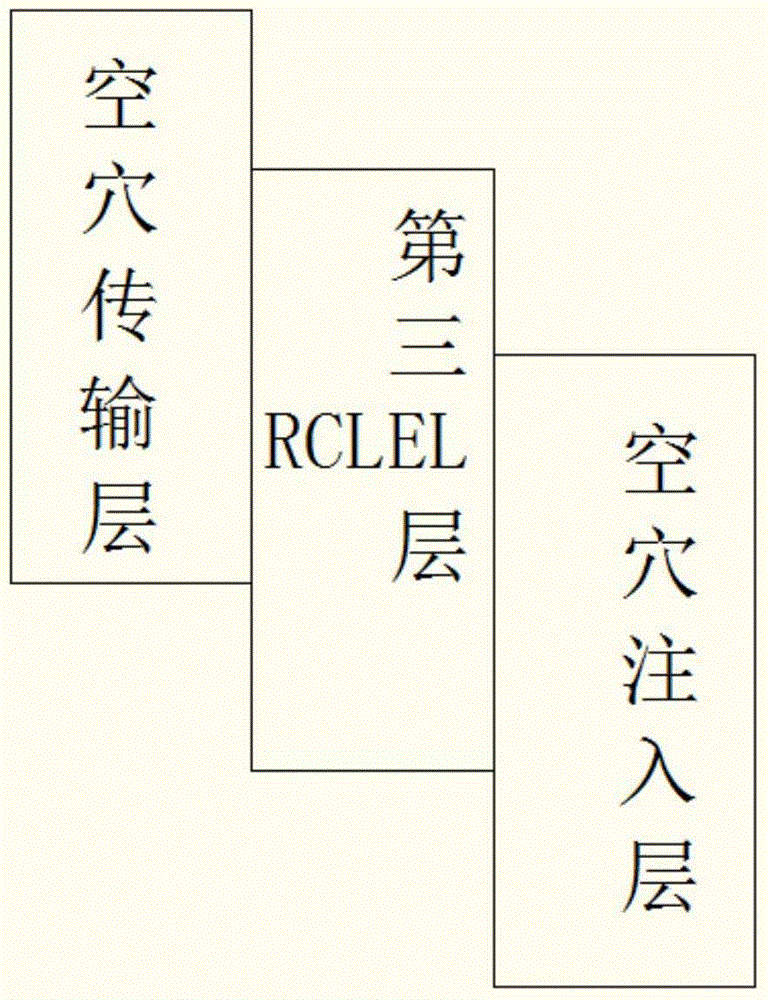
[0030] The core idea of ​​the present invention is to arrange the RCLEL layer between the electron transport layer and the light-emitting layer, and / or the light-emitting layer and the hole transport layer, and / or the hole injection layer and the hole transport layer, due to the electron mobility of the RCLEL layer Faster, it can prevent the accumulation of electrons at the interface of each layer, thereby ensuring the balance of electrons and holes, reducing the formation of recombination centers that do not emit light, thereby improving the life of the device.

[0031] Such as Figure 1a-1c As shown, the present invention has designed a kind of OLED device, and this OLED device comprises electron transport layer, light-emitting layer, hole transport layer and hole injection layer stacked in seq...


PUM


Abstract

The invention relates to the technical field of a semiconductor, and particularly to an OLED device. An RCLEL layer is arranged between an electron transport layer and a hole transport layer; the RCLEL layer can effectively prevent accumulation of electric charges in a film layer interface between the electron transport layer and the hole transport layer, so that a condition that a non-luminous center is formed on the film layer interface caused by the accumulated electric charges is prevented; in addition, the RCLEL layer also has a reversible electrochemical oxidization reduction property, so that material deterioration caused in the transport process of electrons and holes can be greatly relieved; and diffusible ions and impurities also can be effectively prevented from entering a luminous layer, so that the service life of the device is prolonged.

Description

technical field [0001] The invention relates to the technical field of semiconductors, in particular to an OLED device. Background technique [0002] OLED, organic light-emitting diode, has self-illumination, simple structure, ultra-thin, fast response, wide viewing angle, low power consumption and flexible display lamp characteristics. It is known as "dream display" and is considered to be the ideal next generation Flat panel display technology. However, OLED is only used for mobile phones and tablets at present, and its lifespan has always been one of the important factors restricting its application in the TV and vehicle fields. Therefore, improving the lifespan of OLEDs will help expand its application fields. [0003] At present, there are many technologies and structures to improve OLED efficiency and reduce OLED driving voltage, but one of the reasons restricting the wide application of OLED is that its lifespan cannot be compared with that of liquid crystals and LED...

Claims


Application Information

Patent Timeline
Patent Type & Authority Applications(China)
IPC IPC(8): H01L51/50H01L51/54
CPCH10K50/18H10K50/16H10K50/15
Inventor 牟鑫李艳虎王钊张明月
Owner EVERDISPLAY OPTRONICS (SHANGHAI) CO LTD
Why Eureka
Try Eureka