Superconductive nanowire single-photon detector with self-gain structure
A single-photon detector and superconducting nanowire technology, which is applied in the direction of photometry, photometry, and optical radiation measurement using electrical radiation detectors, and can solve problems such as reducing the detection efficiency of superconducting nanowire single-photon detectors. , to achieve self-gain, reduce time-domain jitter, and prevent thermal lock-in effect
- Summary
- Abstract
- Description
- Claims
- Application Information
AI Technical Summary
Problems solved by technology
Method used
Image

Examples
Embodiment 1
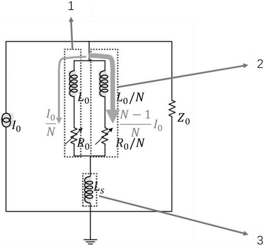
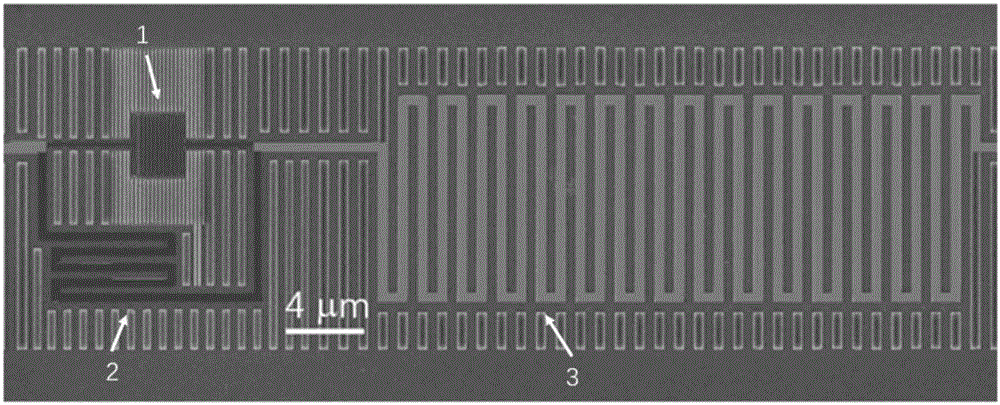
[0032] The circuit diagram of a superconducting nanowire single photon detector (SNSPD) with a self-gain structure is shown in figure 1 As shown, the shape of the nanowire is as figure 2 shown.
[0033] In the embodiment of the present invention, a traditional SNSPD nanowire (that is, the first nanowire 1, used as a photosensitive area) and a nanowire that is thicker than the traditional SNSPD nanowire (that is, the second nanowire 2, As a self-gain region) in parallel, and at the same time connect a thicker nanowire in series (that is, the third nanowire 3, the width of the third nanowire 3 is the sum of the first nanowire 1 and the second nanowire 2, realizing the SNSPD signal self-gain, and reduce the time-domain jitter of SNSPD. By designing the series nanowire (that is, the length of the third nanowire 3 is equivalent to the series inductance L s The length of the inductance value) controls the total inductance of the branch to prevent thermal lock-up effect.
[0034]...
Embodiment 2
[0045] Part of the processing flow of the superconducting nanowire single photon detector with current self-gain structure is as follows:
[0046] 1. Clean the substrate;
[0047] 2. Magnetron sputtering 4-6mm NbN (niobium nitride) thin film;
[0048] 3. Cut the two-inch substrate into small pieces of 1cm×1cm;
[0049] 4. Photolithographic electrodes and alignment marks
[0050] 1) Clean the film (acetone + alcohol + deionized water);
[0051] 2) Spin glue (NR9-3000PY (photoresist), pre-spin 588rpm, 10s, formal spin 2940rpm, 50s);
[0052] 3) Pre-baking (120°C, 5min);
[0053] 4) Exposure (after testing the dose matrix (exposure dose test method));
[0054] 5) Medium drying (95°C, 3min);
[0055] 6) Developing (RD6 (developer solution)), fixing (deionized water).
[0056] 5. Electron beam exposure nanowire + nanowire etching
[0057] 1) Spin gel (HSQ (electron beam exposure glue), pre-spin 588rpm, 10s, formal spin 3528rpm, 100s);
[0058] 2) Pre-baking (90°C, 1min); ...
Embodiment 3
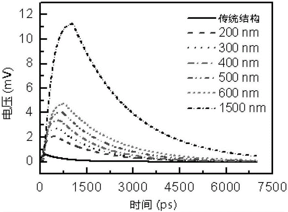
[0065] The embodiment of the present invention uses the electrothermal model to simulate the pulse waveform of the superconducting nanowire single photon detector with the current self-gain structure, and compares and analyzes the superconducting nanowire single photon detector with the current self-gain structure of different widths. The model simulation results are as follows:
[0066] Depend on Figure 3 to Figure 6 It can be seen that with the increase of the width of the self-gain region, although the rise time and recovery time of the pulse are getting longer and longer, the slope at half of the rising edge not only does not decrease, but continues to increase. For the same noise amplitude, the larger the slope corresponding to half of the rising edge, the smaller the time domain jitter. Therefore, the SNSPD with self-gain structure can reduce the time domain jitter, which verifies the feasibility of this method.
[0067] Depend on Figure 7 It can be seen that the ou...
PUM
 Abstract
Description
Claims
Application Information
PatSnap Eureka turns technology decisions into work you can execute. Powered by our Innovation Knowledge Graph, it runs expert workflows across engineering, life sciences, materials and intellectual property. Get your review-ready output in minutes.


