Memristor

A memristor and dielectric layer technology, applied in the field of microelectronics, can solve problems such as difficulty in ensuring the cycle stability and fatigue resistance of synaptic devices, and changes in material microstructures, and achieve excellent cycle stability, low operating voltage, and improved Effect of Controllability and Anti-Fatigue Properties

Inactive Publication Date: 2017-01-04
NINGBO INST OF MATERIALS TECH & ENG CHINESE ACADEMY OF SCI
View PDF7 Cites 26 Cited by
  • Summary
  • Abstract
  • Description
  • Claims
  • Application Information

AI Technical Summary

Problems solved by technology

However, a large operating voltage will inevitably lead to changes in the microstructure of the material

Method used


Image

  • Memristor
  • Memristor
  • Memristor

Examples


Embodiment 1

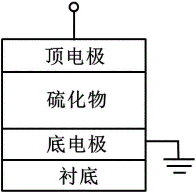
[0034] A memristor, comprising sequentially forming a bottom electrode layer and an intermediate dielectric layer on a substrate, forming a top electrode on the intermediate dielectric layer, and the material of the intermediate dielectric layer is sulfide heat-treated in an oxidizing atmosphere. In this embodiment, the bottom electrode layer is made of metal platinum film; the middle dielectric layer is made of ZnS film heat-treated in an oxidizing atmosphere, and its thickness is 90 nm; the top electrode layer is made of metal copper film, and its thickness is 50 nm.

[0035] The preparation method of the neurosynaptic bionic electronic device (memristive device) of the present embodiment comprises the following steps:

[0036] (1) A 20nm-thick titanium film and a 100nm-thick platinum film were sequentially prepared on the surface of the substrate by electron beam evaporation as the conductive layer, namely the bottom electrode layer.

[0037]The aforementioned substrate is ...

Embodiment 2

[0053] The difference from Example 1 is that the thickness of the intermediate dielectric layer is 30 nm.

Embodiment 3

[0055] The difference from Embodiment 1 is that the thickness of the intermediate dielectric layer is 120 nm.


PUM

PropertyMeasurementUnit
Thicknessaaaaaaaaaa
Thicknessaaaaaaaaaa
Thicknessaaaaaaaaaa

Abstract

The invention provides a memristor. The memristor comprises a bottom electrode layer and an intermediate dielectric layer, wherein the bottom electrode layer and the intermediate dielectric layer are sequentially formed on a substrate, a top electrode is formed on the intermediate dielectric layer, and a material of the intermediate dielectric layer is a sulfide after being subjected to thermal processing in an oxidation atmosphere. The appropriate tope electrode and the sulfide subjected to thermal processing in the oxidation atmosphere are combined, thus the memristor is endowed with many excellent performances such as cycle stability, fatigue resistance and ultralow working voltage; the memristor shows favorable synaptic plasticity in an aspect of biological neural synaptic simulation, and short-range plasticity and long-range plasticity are achieved when the memristor is under the ultralow working voltage (6mV); and the change of an internal structure of the device is reduced due to the ultralow working voltage, thus, the time retentivity and the fatigue resistance of the device are greatly improved, and the power consumption of the device is substantially reduced.

Description

technical field [0001] The invention relates to the technical field of microelectronics, in particular to a memristor. Background technique [0002] Memristor (memristor) is the fourth basic passive electronic device besides resistors, capacitors, and inductors. "Cai Shaotang" first deduced the existence of this element when studying the relationship between charge, current, voltage and magnetic flux in the 1970s, and pointed out that it represented the relationship between charge and magnetic flux. Memristors have the dimension of resistance, but have nonlinear electrical properties different from ordinary resistors. A memristor's resistance changes in response to the amount of charge flowing through it, and it maintains its resistance when the current is turned off. The resistance value of this current-controlled memristive system satisfies a certain mathematical relationship with the applied voltage and time. However, an ideal device with this mathematical relationship ...

Claims


Application Information

Patent Timeline
IPC IPC(8): H01L45/00
CPCH10N70/24H10N70/8822H10N70/041
Inventor 诸葛飞胡令祥曹鸿涛
Owner NINGBO INST OF MATERIALS TECH & ENG CHINESE ACADEMY OF SCI
Why Eureka
Try Eureka