

Method for substrate epitaxial growth of luminous diode based on AlN template
A light-emitting diode and epitaxial growth technology, which is applied in the direction of electrical components, circuits, semiconductor devices, etc., can solve the problems of low wavelength hit rate, poor antistatic ability, and low brightness of epitaxial wafers, so as to improve production efficiency and simplify epitaxial growth Effect
- Summary
- Abstract
- Description
- Claims
- Application Information
AI Technical Summary
Problems solved by technology
Method used
Image

Examples
Embodiment 1
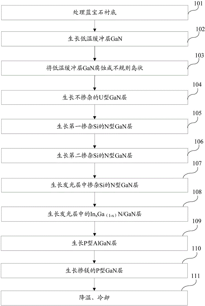
[0065] like image 3 As shown, it is a schematic flow chart of the method for epitaxial growth of light-emitting diode substrates based on AlN templates described in this embodiment. The method described in this embodiment solves the problem of the method for preparing LEDs in the prior art so that the wavelength hit rate of the prepared epitaxial wafers Low, epitaxial wafer crystal quality is light, the crystal quality of the light-emitting layer is poor, the doping efficiency of the P layer is reduced, and the mobility of the holes is reduced; resulting in a decrease in brightness, a decrease in luminous efficacy, a decrease in reverse voltage, and an antistatic ability of the prepared LED Bad question.
[0066] In this embodiment, MOCVD (metal organic compound chemical vapor deposition) is used to grow high-brightness GaN-based LED epitaxial wafers, using high-purity H 2 or high purity N 2 or high purity H 2 and high purity N 2 The mixed gas as the carrier gas, high-pur...
Embodiment 2
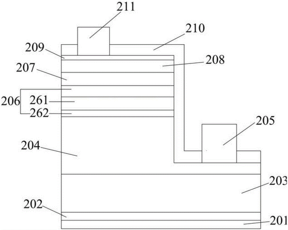
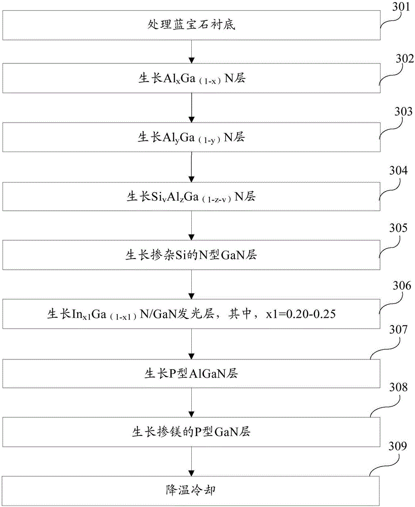
[0082] like Figure 3-5 as shown, Figure 5 It is a schematic flowchart of the method for epitaxial growth of a light-emitting diode substrate based on an AlN template described in this embodiment. On the basis of Example 1, the specific content of the overall growth of an epitaxial layer of a light-emitting diode based on an AlN template is described. The method for the epitaxial growth of a light-emitting diode substrate based on an AlN template described in this embodiment includes the following steps:
[0083] Step 501, processing the sapphire substrate: Into the reaction chamber of the metal-organic chemical vapor deposition system with the substrate placed, NH with a flow rate of 10000-20000 sccm is introduced at the same time 3 , 100-130L / min H 2 , increasing the temperature to 900-1000° C., and processing the substrate for 300s-600s under the condition that the reaction chamber pressure is 100-200mbar.
[0084] Step 502, growing Al x Ga (1-x) N layers, further:
...
Embodiment 3
[0100] In this embodiment, LED sample 1 was prepared according to the traditional LED growth method, and sample 2 was prepared according to the LED growth method of the present invention; parameters of the epitaxial growth methods of sample 1 and sample 2 are shown in Table 1. Put sample 1 and sample 2 into XRD measuring equipment (X-ray Diffraction, also known as X-ray diffractometer) at the same time to measure the value of GaN layer and the value of luminescence layer, see Table 3 for details. Then sample 1 and sample 2 are plated with about 150nm thick ITO layer under the same pre-process conditions; plated with about 1500nm of Cr / Pt / Au electrodes under the same conditions; The protective layer of SiO 2 , and then grind and cut the sample into chip particles of 635μm*635μm (25mil*25mil) under the same conditions, then select 100 grains from sample 1 and sample 2 at the same position, and package them into White LEDs. The photoelectric properties of sample 1 and sample 2 ...
PUM
| Property | Measurement | Unit |
|---|---|---|
| Light effect | aaaaa | aaaaa |
Abstract
Description
Claims
Application Information