Low-thermal-resistance radiation-resistant nano multilayer film material and preparation method thereof

A nano-multi-layer and thin-film material technology, applied in the field of nano-materials, can solve problems such as thermal performance degradation, achieve low interface contact thermal resistance, reduce thermal conductivity degradation, and excellent radiation resistance

Active Publication Date: 2017-01-25
WUHAN UNIV
View PDF1 Cites 6 Cited by
  • Summary
  • Abstract
  • Description
  • Claims
  • Application Information

AI Technical Summary

Problems solved by technology

[0003] In recent years, bimetallic nano-multilayer film materials containing a large number of interfaces and grain boundaries, which can greatly reduce the damage caused by radiation, have been widely studied and recognized, but the design of this multilayer film has led to a cliff in the thermal properties of the material. Therefore, in the face of high-temperature, high-irradiation nuclear reaction environment, it is imperative to develop a material with good thermal conductivity and radiation resistance.

Method used


Image

  • Low-thermal-resistance radiation-resistant nano multilayer film material and preparation method thereof
  • Low-thermal-resistance radiation-resistant nano multilayer film material and preparation method thereof
  • Low-thermal-resistance radiation-resistant nano multilayer film material and preparation method thereof

Examples


Embodiment 1

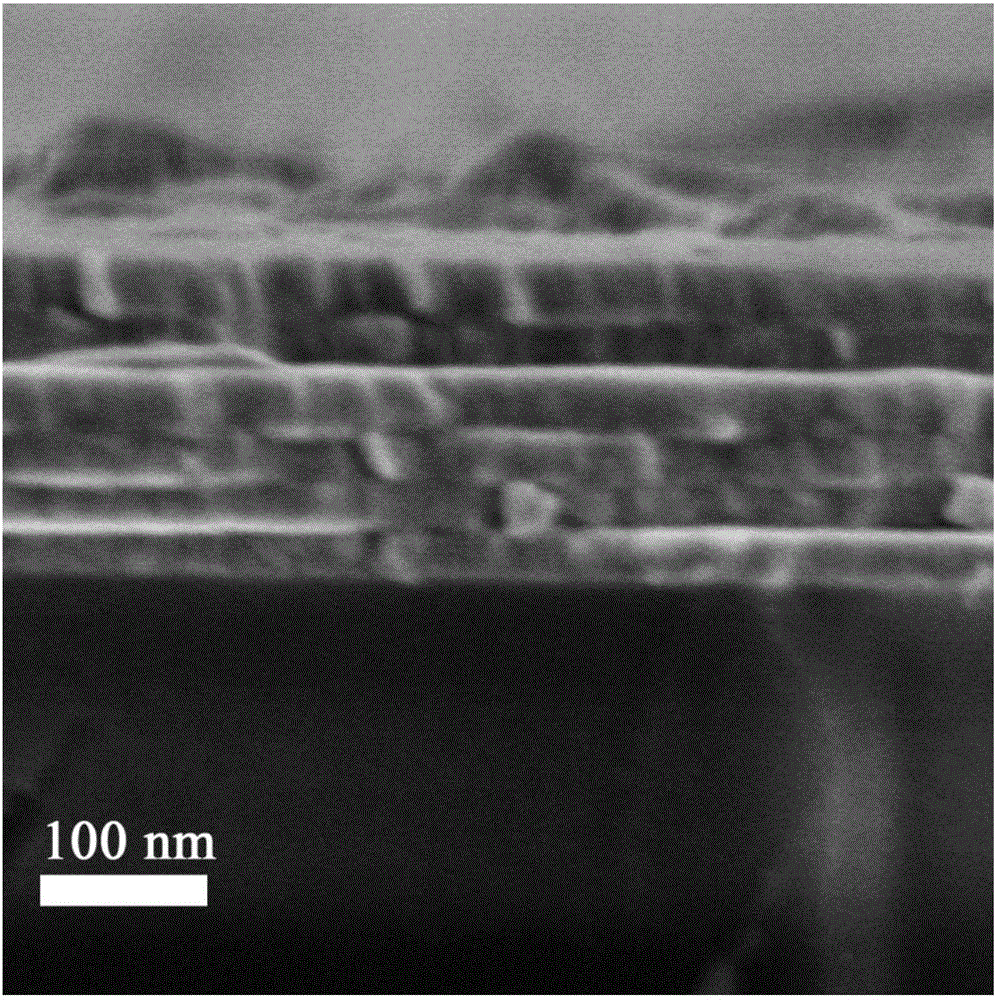
[0035] A low thermal resistance, radiation-resistant nano-multilayer film material, which is a multi-layer composite structure cross-stacked with metal tungsten nano-film and single-layer graphene; wherein, the thickness of the metal tungsten nano-film is 30nm, and the number of layers is 6 layers, and the number of layers of single-layer graphene is 5 layers.

[0036] The preparation method of the above-mentioned low thermal resistance, radiation-resistant nanometer multi-layer thin film material specifically comprises the following steps:

[0037] (1) Sonicate the 300nm silicon dioxide substrate with acetone, absolute ethanol, and deionized water for 10 minutes in sequence, then dry it with a nitrogen gun, and then use a magnetron sputtering system to deposit a layer of metal tungsten nano-film; wherein, the magnetron Sputtering parameters: sputtering voltage 150w, background vacuum lower than 10 -4 pa, the film-forming vacuum is 0.5pa, the argon gas flow is 20sccm, and the...

Embodiment 2

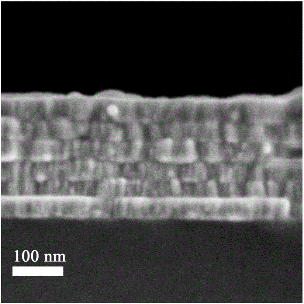
[0044] The differences between this embodiment and Embodiment 1 are: the thickness of each layer of metallic tungsten nano film is 40 nm; the magnetron sputtering time is 10 min.

[0045]Measure the low thermal resistance and radiation-resistant nano-multilayer film material obtained in this embodiment by photothermal method measurement technology, wherein the number of layers of metal tungsten nano-film is 6 layers, and the number of layers of single-layer graphene is 5 layers. The thermal resistance caused by adding the graphene layer is 17.92×10 -9 Km 2 W -1 . This means that the thermal resistance caused by the graphene interface is very small and hardly hinders the transfer of heat, and the material obtained in this embodiment shows excellent thermal conductivity.

Embodiment 3

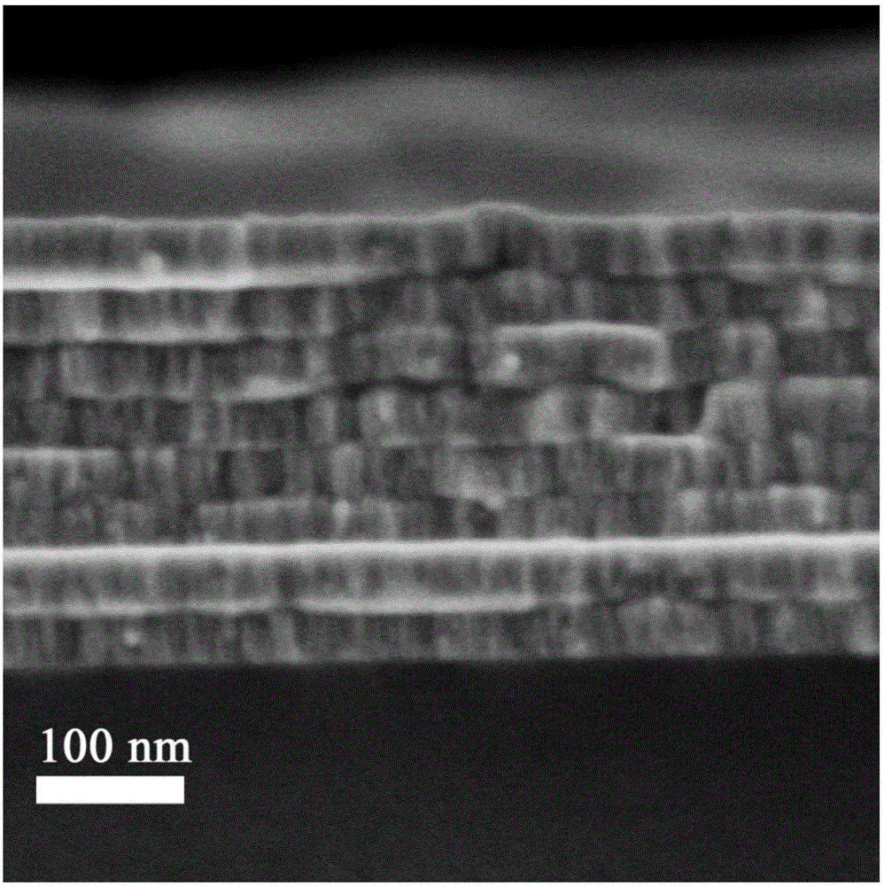
[0047] The difference between this embodiment and Example 1 is: the thickness of each layer of metal tungsten nano film is 40nm; the magnetron sputtering time is 10min, so that the thickness of each layer of metal tungsten nano film is 40nm; step (4) is a cycle repeating step (2) and (3) 6 times; the obtained low thermal resistance, radiation-resistant nano-multilayer film material, wherein 8 layers of metal tungsten nano-film, 7 layers of single-layer graphene.

[0048] Measure the nano-multilayer film material with low thermal resistance and radiation resistance obtained in this embodiment by photothermal method measurement technology, wherein the number of layers of metal tungsten nano-film is 8 layers, and the number of layers of single-layer graphene is 7 layers. The thermal resistance caused by the graphene layer is 10.29×10 -9 Km 2 W -1 . This means that the thermal resistance caused by the graphene interface is very small and hardly hinders the transfer of heat, and...


PUM

PropertyMeasurementUnit
thicknessaaaaaaaaaa
thicknessaaaaaaaaaa
thicknessaaaaaaaaaa

Abstract

The invention discloses a low-thermal-resistance radiation-resistant nano multilayer film material. The material has a multilayer composite structure formed by cross stacking of metal tungsten nano films and single-layer graphene. A preparation method of the material comprises the following steps: depositing a metal tungsten nano film on a silicon dioxide substrate; transferring single-layer graphene onto the surface of the metal tungsten nano film; and alternately depositing a metal tungsten nano film and transferring single-layer graphene to obtain the low-thermal-resistance radiation-resistant nano multilayer film material. Aiming at the problem that the present bimetal multilayer film structure can greatly lower the thermal property of the material, the material provided by the invention integrates excellent heat-conducting property and radiation resistance and has the multilayer composite structure formed by cross stacking of metal tungsten nano films and single-layer graphene, so that the thermal conductivity lowering caused by the presence of a multilayer film structural interface can be reduced, and the excellent radiation resistance of the material can be kept.

Description

technical field [0001] The invention belongs to the field of nanometer materials, and relates to a nanometer multilayer film material with low thermal resistance and radiation resistance and a preparation method thereof. Background technique [0002] Energy is the basis for the survival and development of human beings, and it constantly promotes the continuous progress of human society. After entering the 21st century, with the rapid development of modern society, the demand and consumption of energy have increased significantly, and the constraints of energy and the environment on social development have become increasingly prominent. As a new type of clean energy, nuclear power generation has significant advantages such as low resource consumption, low environmental impact, and strong supply capacity. It has attracted more and more attention from the international community. Nuclear power has become an important choice for many countries' energy strategies. One of the eff...

Claims


Application Information

Patent Timeline
Patent Type & Authority Applications(China)
IPC IPC(8): C23C14/18C23C14/35C23C28/00C23C16/01C23C16/26
CPCC23C14/185C23C14/35C23C16/01C23C16/26C23C28/322C23C28/343C23C28/42
Inventor 肖湘衡司书尧赵晓龙李文庆蒋昌忠
Owner WUHAN UNIV
Why Eureka
Try Eureka