Method using laser interference to induce electrochemical deposition so as to prepare periodic and patterned Fe3O4 nano particles

A technology of laser interference and nano-particles, which is applied in nano-technology, electrodes, electrolytic coatings, etc., can solve the problems that nano-materials cannot meet the needs of performance research, fine application, rough particle size distribution, etc., and achieve low preparation costs, simple equipment, and raw materials. Easy to get effect

Active Publication Date: 2017-01-25
CHANGCHUN UNIV OF SCI & TECH
1 Cites 11 Cited by

AI-Extracted Technical Summary

Problems solved by technology

[0003] Currently about magnetic Fe 3 o 4 There are many methods for the preparation of nanoparticles, which are divided into physical methods and chemical methods. Due to the shortcomings of the particle size distribution of the nanoparticles prepared by the physical method, the prepared nanomaterials cannot meet the needs of p...

Abstract

The invention relates to a method using laser interference to induce electrochemical deposition so as to prepare periodic and patterned Fe3O4 nano particles. The method is characterized in that the light-induced dielectrophoresis and electrochemical deposition technologies are used, a laser interference light source is used as the induction light source, an ITO conductive substrate plated with hydrogenated amorphous silicon thin film is used as the working electrode, a saturated calomel electrode is used as the reference electrode, a high-purity iron sheet is used as the counter electrode, the mixed solution of FeCl2 and FeCl3 is used as the electrolyte, the induction light source is projected to the hydrogenated amorphous silicon thin film, and a photoelectric effect is used to allow an exposure part to generate a virtual electrode; chronoamperometry is used to perform electrochemical deposition on the virtual electrode to generate the Fe3O4 nano particles, and an ordered Fe3O4 nano particle array consistent with a laser interference pattern is obtained. The method has the advantages that the method is simple in equipment and low in preparation cost, high-temperature heating or annealing is not needed, used chemicals are nontoxic and harmless, and the prepared patterned ordered Fe3O4 nano particle array is good in reproducibility and stability.

Application Domain

Electrolytic inorganic material coatingElectrophoretic coatings +2

Technology Topic

ChronoamperometryLaser interference +9

Image

  • Method using laser interference to induce electrochemical deposition so as to prepare periodic and patterned Fe3O4 nano particles
  • Method using laser interference to induce electrochemical deposition so as to prepare periodic and patterned Fe3O4 nano particles
  • Method using laser interference to induce electrochemical deposition so as to prepare periodic and patterned Fe3O4 nano particles

Examples

  • Experimental program(1)

Example Embodiment

[0033] The present invention will be described in detail below with reference to specific embodiments.
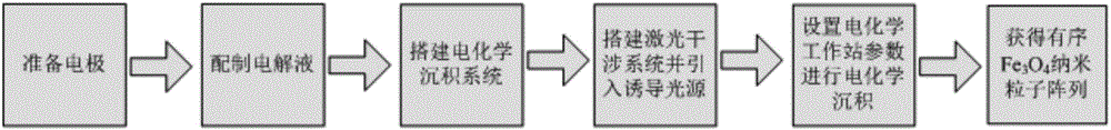
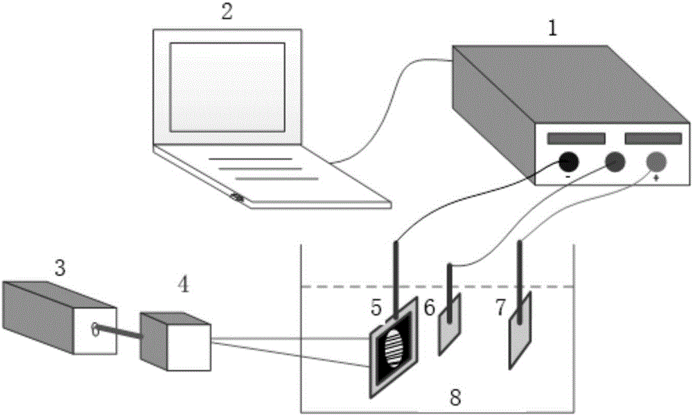
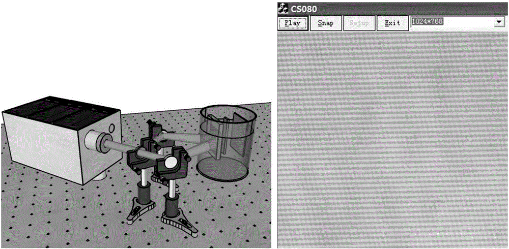
[0034] like figure 1 As shown, the present invention adopts a simple laser interference-induced electrochemical deposition to prepare patterned Fe 3 O 4 The nanoparticle approach is as follows:
[0035] (1) Preparation of electrodes: the ITO conductive substrate coated with hydrogenated amorphous silicon (a-Si:H) thin film was used as the working electrode; the high-purity iron sheet was used as the counter electrode; and the calomel electrode was used as the reference electrode. The surface area of ​​the ITO conductive substrate is 1 cm 2 , the square resistance is 4Ω, the thickness of the ITO film is 500nm, and the transmittance is 84%; the hydrogenated amorphous silicon (a-Si:H) film is deposited on the surface of ITO by PECVD method, the thickness is 500nm, and the dark state conductivity is 5E- 10S/cm, the photoconductivity under AM1.5G illumination is about 7E-5S/cm. Among them, the ITO with a width of 2 mm left on the edge of the ITO does not deposit a hydrogenated amorphous silicon (a-Si:H) film, which is used as a lower conductive electrode.
[0036] (2) Preparation of electrolyte: use ferric chloride hexahydrate as the ferric iron source, prepare 12mM FeCl 3 50ml of deionized water solution, using ferric chloride tetrahydrate as the divalent iron source to prepare 8mM FeCl 2 50ml of deionized aqueous solution; ultrasonically dissolve the two solutions respectively, and ultrasonically dissolve again after mixing to obtain an electrolyte solution, FeCl 3 with FeCl 2 The molar ratio is 3:2.
[0037] (3) Set up an electrochemical deposition system: place 100 ml of the electrolyte prepared in (2) in a square quartz beaker with a capacity of 150 ml, soak the three-phase electrode prepared in step (1) in the electrolyte, and place the ITO electrode in the electrolyte. On the outermost side, the uncoated side faces the beaker wall, and the hydrogenated amorphous silicon (a-Si:H) thin film is plated towards the inside of the beaker. like figure 2 As shown, the system of the present invention includes an electrochemical workstation 1, a computer 2, a laser light source 3, an interference system 4, an ITO electrode 5 coated with a hydrogenated amorphous silicon (a-Si:H) thin film, a calomel electrode 6, a high-purity iron Sheet 7, FeCl 3 and FeCl 2 Solution 8. The electrochemical workstation 1 is connected with the computer 2, the laser light source 3 is incident on the interference system 4, and the ITO electrode 5, the calomel electrode 6, and the high-purity iron sheet 7 coated with the hydrogenated amorphous silicon (a-Si:H) film are placed. In FeCl3 and FeCl2 solution 8, the negative electrode of electrochemical workstation 1 is connected with ITO electrode 5 coated with hydrogenated amorphous silicon (a-Si:H) film, the reference electrode is connected with calomel electrode 6, and the positive electrode is connected with high-purity iron Slice 7 is connected.
[0038] (4) Build a laser interference system and introduce an induced light source: Select a 457nm wavelength laser as the interference light source, build a 5μm periodic wire grid laser interference system, obtain a 5μm periodic wire grid induced light source, and introduce the light source to the ITO working electrode to adjust the optical path The interference light source was projected onto the hydrogenated amorphous silicon (a-Si:H) thin film through the beaker, the solution and the ITO substrate. The photoelectric effect generated when the induced light source is projected on the backside of the hydrogenated amorphous silicon (a-Si:H) thin film makes the exposed part of the hydrogenated amorphous silicon (a-Si:H) thin film generate a large number of photogenerated carriers and reduces the impedance, thereby reducing the impedance. A wire grid dummy electrode with a period of 5 μm was generated.
[0039] like image 3 As shown in the left figure of the present invention, the interference of two beams realizes Fe 3 O 4 Schematic diagram of the laser interferometry system fabricated by the nanoparticle array. The laser interference system used is composed of a high-reflection mirror and a beam splitter. A laser beam emitted by the laser is divided into two beams of coherent beams by a beam splitter, and the two beams of coherent beams are made spatially symmetrical by the reflection system, and they are simultaneously irradiated to the hydrogenated amorphous silicon (a-Si:H) film at a certain incident angle , forming a 5μm wire grid induced light source, such as image 3 Shown on the right.
[0040] (5) Set the electrochemical workstation parameters for electrochemical deposition: at room temperature, use CHI660D electrochemical workstation to control the cathode current density of 2 mA/cm 2 In condition 1) deposition time 50s and laser power density 2mW/cm 2;2) Deposition time 100s and laser power density 5mW/cm 2;3) Deposition time 200s and laser power density 10mW/cm 2; Electrochemical deposition was performed. After the operation, the power was turned off to take out the working electrode, rinsed with deionized water three times, and air-dried at room temperature to obtain samples 1, 2 and 3.
[0041] (6) Test the sample piece 1 with a scanning electron microscope SEM, that is, to obtain a nanoparticle wire grid with a period of 5 μm attached to the hydrogenated amorphous silicon thin film. like Figure 4 shown, the wire grid pattern Fe prepared for the two-beam interference 3 O 4 The SEM image of the nanoparticle array, the left image is the distribution map of the large-area periodic wire grid, and the right image is the enlarged image of the multi-periodic wire grid. The deposited periodic wire grid pattern Fe can be seen 3 O 4 The nanoparticle array period is 5 μm with image 3 The 5μm wire grid fringes formed by the double-beam laser interference system induce the same light source.
[0042] (7) The nanoparticles in the samples 1, 2 and 3 were tested with a scanning electron microscope SEM, and the results were as follows: Figure 5 shown, Fe with different particle size and morphology 3 O 4 SEM image of nanoparticles, in which the left pattern sheet 1 is hexahedral and triangular pyramid; the middle pattern sheet 2 is snowflake shape; the right pattern sheet 3 is scaly layered, with the deposition time from 50s-200s, laser power density from 2mW/cm 2 -10mW/cm 2 Variation, Fe as prepared 3 O 4 The particle size becomes larger and the shape changes.
[0043] (8) Test sample 1 with an X-ray diffractometer, such as Image 6 Shown is the X-ray diffraction pattern of the deposited sample, the abscissa 9 is the 2θ angle (degrees), and the ordinate 10 is the intensity. Among them, the four main peaks and Fe 3 O 4 The standard spectrum is consistent, and the main component of the nanoparticles is determined to be Fe 3 O 4.

PUM

no PUM

Description & Claims & Application Information

We can also present the details of the Description, Claims and Application information to help users get a comprehensive understanding of the technical details of the patent, such as background art, summary of invention, brief description of drawings, description of embodiments, and other original content. On the other hand, users can also determine the specific scope of protection of the technology through the list of claims; as well as understand the changes in the life cycle of the technology with the presentation of the patent timeline. Login to view more.

Similar technology patents

Process for preparing notoginsen triterpenes

InactiveCN1634970Aincrease the rate of submissionsimple equipment
Owner:张平

Video anti-shake method based on feature point matching

InactiveCN103813099Asimple equipmentlow cost
Owner:RES INST OF SUN YAT SEN UNIV & SHENZHEN

Classification and recommendation of technical efficacy words

  • simple equipment
  • low cost of preparation

Innocent treatment of cyanide and fluoride in solid waste residues and recycling process thereof

ActiveCN101444660Asimple equipmentreduce land use
Owner:浙江钰滔环保科技有限公司

Telegraph pole installation robot

Owner:浙江邮电职业技术学院 +1

Quadruple frequency-based scheme for realizing base station passive full duplex millimeter wave RoF link

InactiveCN101742738Asimple equipmentStrong practical operability
Owner:BEIJING UNIV OF POSTS & TELECOMM

Preparation of microballoons based on microfluid

InactiveCN101279232Alow cost of preparationEasy integration and miniaturization
Owner:NANJING DONGJIAN BIOLOGICAL TECH

Hydro-fining catalyst roasted at low temperature and preparation method thereof

InactiveCN102784656AImprove activity and stabilitylow cost of preparation
Owner:CHINA UNIV OF PETROLEUM (EAST CHINA)
Why Eureka
Try Eureka