A kind of preparation method of silicon-based heterojunction solar cell and its tinx barrier layer
A heterojunction cell, silicon-based technology, used in circuits, photovoltaic power generation, electrical components, etc., can solve problems such as difficult removal, and achieve the effects of increased adhesion, easy solution corrosion, and low resistivity
- Summary
- Abstract
- Description
- Claims
- Application Information
AI Technical Summary
Problems solved by technology
Method used
Image
Examples
Embodiment 1
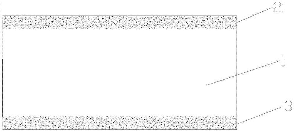
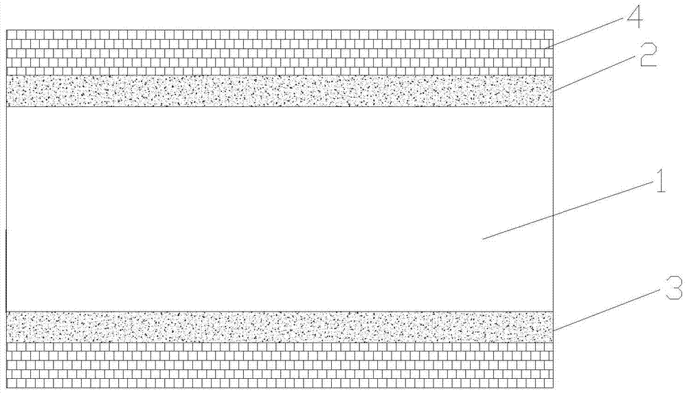
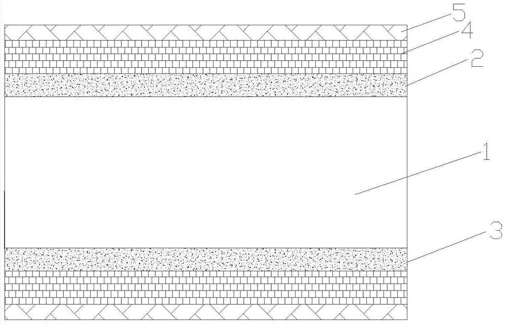
[0027] refer to Figure 1-Figure 6 A silicon-based heterojunction solar cell and its TiN x The preparation method of the barrier layer is mainly by preparing TiN x barrier layer, and the TiN x The barrier layer is applied to the silicon-based heterojunction cell, which includes the following steps:
[0028] Step 1. Deposit an intrinsic amorphous silicon layer and a P-type amorphous silicon thin film layer 2 on the front side of the N-type silicon wafer 1 that has a light-trapping effect after being etched by an alkaline or acidic solution, and deposit an intrinsic amorphous silicon layer on the reverse side. A silicon layer and an N-type amorphous silicon thin film layer 3 .
[0029] Step 2: Deposit a transparent conductive oxide film 4 on the P-type amorphous silicon thin film layer 2 and the N-type amorphous silicon thin film layer 3 by PVD sputtering method, and the transparent conductive oxide thin film 4 is made of ITO.
[0030] Step 3: Depositing TiN on the transpare...
Embodiment 2
[0036] With reference to the preparation steps described in Example 1, the TiN prepared by depositing on the surface of single crystal silicon in this example x After the barrier layer 5, copper plating is carried out, so that the TiN x A layer of copper thin film is formed on the barrier layer 5, and then the silicon wafer is heat-treated at 400°C for 30 minutes. The test results show that no copper-silicon compound is produced, and the diffusion barrier performance is good.
Embodiment 3
[0038] Referring to the preparation steps described in Example 1, the prepared TiN is deposited on the surface of single crystal silicon in this embodiment x Barrier layer 5, the thickness is controllable only between 2-50nm, good uniformity, can ensure the excellent quality of subsequent deposited copper layer, at the same time deposited at low temperature, the film has an amorphous structure, treated in alkaline corrosion solution, 30-120S The inner film is completely etched away, effectively reducing light loss.
PUM
| Property | Measurement | Unit |
|---|---|---|
| purity | aaaaa | aaaaa |
Abstract
Description
Claims
Application Information


