Crystalline silicon cell piece and preparation method thereof

A technology of crystalline silicon cells and crystalline silicon wafers, which is applied in circuits, photovoltaic power generation, electrical components, etc., can solve the problems of poor resistance to high and low temperature cycle changes of welding electrodes, affecting the overall performance of packaging components, and poor consistency.

Active Publication Date: 2017-02-15
48TH RES INST OF CHINA ELECTRONICS TECH GROUP CORP
View PDF5 Cites 4 Cited by
  • Summary
  • Abstract
  • Description
  • Claims
  • Application Information

AI Technical Summary

Problems solved by technology

Electrodes are prepared based on conventional printing silver paste or photolithography. Due to the relatively large square resistance, if resistance welding technology is used, there will be two major problems: 1) The high-temperature sintering temperature of crystalline silicon electrodes is within 880°C, while the peak temperature of resistance welding is generally at Above 900°C, it is very easy for silver to burn through the PN junction, resulting in serious battery leakage; 2) The properties (metal type and content) of the conventional matching silver paste and the silver foil of

Method used


Image

  • Crystalline silicon cell piece and preparation method thereof
  • Crystalline silicon cell piece and preparation method thereof
  • Crystalline silicon cell piece and preparation method thereof

Examples


Embodiment 1

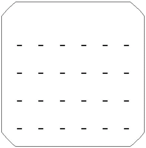
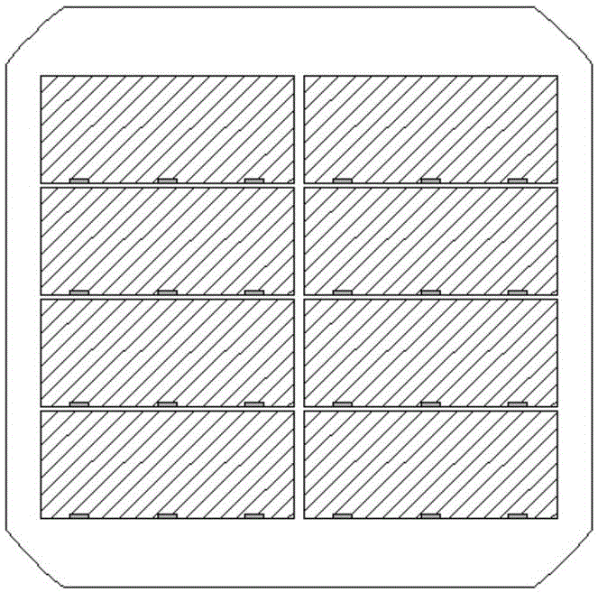
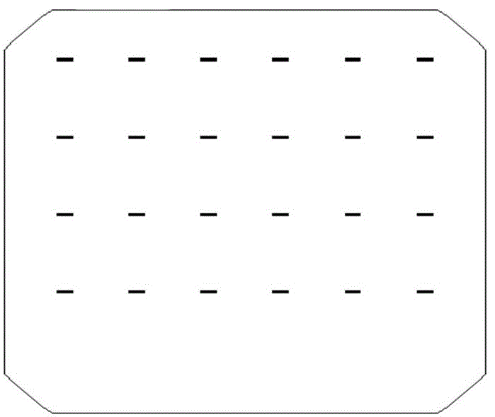
[0037] A crystalline silicon cell of the present invention comprises a crystalline silicon cell substrate, a finger grid electrode, a welding electrode, a back electrode and an aluminum back conductive layer, the finger grid electrode and the welding electrode are arranged on the front of the crystal silicon cell substrate, and the back electrode And the aluminum back conductive layer is arranged on the back of the crystalline silicon cell substrate; wherein, the square resistance value of the area corresponding to the welding electrode on the front of the crystalline silicon cell substrate is 40Ω / □~50Ω / □, and the thickness of the aluminum back conductive layer is thicker than the back electrode 1 μm higher, the thickness of the finger grid electrode is 1 μm higher than that of the welding electrode.

[0038] In this embodiment, the crystalline silicon cell substrate includes SiNx anti-reflection film, SiO 2 Thin films, PN junctions, front textured crystalline silicon wafers, ...


PUM

PropertyMeasurementUnit
Film thicknessaaaaaaaaaa
Meshaaaaaaaaaa

Abstract

The invention discloses a crystalline silicon cell piece and a preparation method thereof. The crystalline silicon cell piece comprises a substrate, a gate electrode, a welding electrode, a back electrode and an aluminum back conductive layer, wherein the gate electrode and the welding electrode are arranged on the front of the substrate, and the back electrode and the aluminum back conductive layer are arranged on the back of the substrate; a square resistance value of an area, corresponding to the welding electrode, of the front of the substrate is 20 omega/square - 60 omega/square, the aluminum back conductive layer is 1 micron - 3 microns thicker than that of the back electrode, and the gate electrode is 1 micron - 3 microns thicker than the welding electrode. The preparation method comprises the following steps of (1) diffusing PN junctions; (2) laser doping; (3) film forming; (4) silk-screen printing and (5) sintering. The crystalline silicon cell piece has the advantages of being high in tolerance for welding temperature, not prone to generate electric leakage, and good in packaging performance; the preparation method is low in cost and beneficial to industrial production, and has the advantage of higher cost performance in the field of spaceflight cells for commercial satellites.

Description

technical field [0001] The invention belongs to the field of production and manufacture of solar crystalline silicon cells, and in particular relates to a crystalline silicon cell and a preparation method thereof. Background technique [0002] Solar cell modules for space vehicles not only require high conversion efficiency, but also require high-altitude environmental characteristics such as resistance to atomic oxygen corrosion, low air pressure, and strong vibration. With good environmental adaptability, crystalline silicon cells and gallium arsenide cells have long served space vehicles. With the continuous advancement of multi-junction gallium arsenide battery manufacturing technology, its photoelectric conversion efficiency rapidly exceeds that of crystalline silicon batteries. Since the Shenzhou 7 spacecraft, gallium arsenide batteries have become the first choice for the Shenzhou spacecraft, but the price of gallium arsenide batteries is much higher For crystalline ...

Claims


Application Information

Patent Timeline
IPC IPC(8): H01L31/048H01L31/18H01L31/0224
CPCH01L31/022441H01L31/048H01L31/1804Y02E10/50Y02P70/50
Inventor 姬常晓张建国杨晓生周洪彪
Owner 48TH RES INST OF CHINA ELECTRONICS TECH GROUP CORP
Why Eureka
Try Eureka