Quantum dot light-doped graphene/boron nitride/gallium nitride ultraviolet detector and manufacturing method thereof

A technology of graphene and quantum dots, which is applied in quantum dot light-doped graphene/boron nitride/gallium nitride ultraviolet photodetectors and its preparation, and in the field of ultraviolet photodetectors and their preparation, which can solve the problem of affecting the detector light. Problems such as detection responsivity and detection degree, to achieve good light absorption and light detection response performance, easy to implement, and high carrier mobility

Active Publication Date: 2018-11-13
ZHEJIANG UNIV
View PDF7 Cites 0 Cited by
  • Summary
  • Abstract
  • Description
  • Claims
  • Application Information

AI Technical Summary

Problems solved by technology

But at the same time, considering that graphene is only atomically nanometer-level thick, it absorbs relatively little light (~2.3%), which will affect the photodetection responsivity and detectability of the detector.

Method used


Image

  • Quantum dot light-doped graphene/boron nitride/gallium nitride ultraviolet detector and manufacturing method thereof
  • Quantum dot light-doped graphene/boron nitride/gallium nitride ultraviolet detector and manufacturing method thereof
  • Quantum dot light-doped graphene/boron nitride/gallium nitride ultraviolet detector and manufacturing method thereof

Examples


Embodiment 1

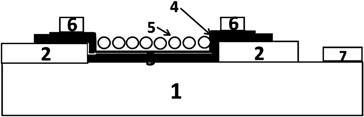
[0022] 1) On the front side of the N-type doped sapphire substrate gallium nitride wafer, make a side electrode in a certain area, the material is 100nm nickel / gold electrode, and the area accounts for about 5% of the entire front gallium nitride substrate, and then Immerse in acetone and isopropanol solutions successively for surface cleaning, wash with deionized water, take out and dry;

[0023] 2) A layer of 80nm silicon nitride (SiN x ) an insulating layer, the area of ​​which is about 80% of the entire GaN substrate, and a certain area (2mm*2mm) is left in the middle area of ​​the insulating layer without an insulating layer, that is, a window;

[0024] 3) transferring the single-layer graphene to boron nitride, the area of ​​boron nitride is larger than the area of ​​single-layer graphene and larger than the blank area in the middle of the insulating layer, and the thickness of the boron nitride is 5nm;

[0025] 4) transfer the boron nitride on which the graphene is tra...

Embodiment 2

[0029] 1) On the front side of the N-type doped sapphire substrate gallium nitride wafer, make a side electrode in a certain area, the material is 100nm chromium / gold electrode, and the area accounts for about 5% of the entire front gallium nitride substrate, and then Immerse in acetone and isopropanol solutions successively for surface cleaning, wash with deionized water, take out and dry;

[0030] 2) A layer of 80nm silicon nitride (SiN x ) an insulating layer, the area of ​​which is about 90% of the entire gallium nitride substrate, and a certain area (1mm*1mm) is left in the middle area of ​​the insulating layer without an insulating layer;

[0031] 3) transferring single-layer graphene to boron nitride requires that the area of ​​boron nitride be larger than the area of ​​single-layer graphene and larger than the blank area in the middle of the insulating layer;

[0032] 4) transfer the boron nitride on which the graphene is transferred as a whole to the above-mentioned ga...

Embodiment 3

[0035] 1) On the front side of the N-type doped sapphire substrate gallium nitride wafer, make a side electrode in a certain area, the material is 200nm chromium / gold electrode, and the area accounts for about 5% of the entire front gallium nitride substrate, and then Immerse in acetone and isopropanol solutions successively for surface cleaning, wash with deionized water, take out and dry;

[0036] 2) A layer of 80nm silicon nitride (SiN x ) an insulating layer, the area of ​​which is about 90% of the entire gallium nitride substrate, and a certain area (1mm*1mm) is left in the middle area of ​​the insulating layer without an insulating layer;

[0037] 3) Transferring three layers of graphene to boron nitride requires that the area of ​​boron nitride be larger than the area of ​​single-layer graphene and larger than the blank area in the middle of the insulating layer;

[0038] 4) transfer the boron nitride on which the graphene is transferred as a whole to the above-mention...


PUM

PropertyMeasurementUnit
diameteraaaaaaaaaa
thicknessaaaaaaaaaa
thicknessaaaaaaaaaa

Abstract

The invention discloses a quantum dot-photodoped graphene / boron nitride / gallium nitride ultraviolet photoelectric detector. A sapphire substrate is sequentially provided with an N-type doped gallium nitride layer, an insulating layer, a boron nitride layer, a graphene layer and a quantum dot layer from bottom to top, and is provided with a first electrode and a side electrode. The preparation method comprises the steps of firstly manufacturing the side electrode and the insulating layer on an N-type doped sapphire substrate gallium nitride wafer and reserving a window in the insulating layer; transferring graphene to boron nitride, transferring the boron nitride to the insulating layer and making the boron nitride in the window in contact with gallium nitride to form a heterojunction; and manufacturing a first electrode on the graphene and carrying out photodoping on the graphene by using quantum dots to obtain the quantum dot-photodoped graphene / boron nitride / gallium nitride ultraviolet photoelectric detector. According to the ultraviolet photoelectric detector disclosed by the invention, photodoping is carried out on the graphene through the quantum dots, so that the performance of a device is further optimized, the dark current is low, the ultraviolet photoelectric detector has extremely high responsivity and detectivity on an ultraviolet band and the process of the device is simple.

Description

technical field [0001] The invention relates to an ultraviolet photodetector and a preparation method thereof, in particular to a quantum dot light-doped graphene / boron nitride / gallium nitride ultraviolet photodetector and a preparation method thereof, belonging to the technical field of optoelectronic devices. Background technique [0002] In recent years, ultraviolet detectors, as an important optoelectronic device, have attracted extensive attention from research and industry. Among them, photodetectors with two-dimensional material / semiconductor heterojunction structures have attracted more and more researchers for their extremely fast response, high responsivity and detection performance, and can be widely used in aviation and military applications. field. [0003] After the graphene material was first discovered and prepared in 2004 and won the Nobel Prize in 2010, its research has made faster progress. More studies have shown that graphene materials have excellent e...

Claims


Application Information

Patent Timeline
Patent Type & Authority Patents(China)
IPC IPC(8): H01L31/0352H01L31/109H01L31/18
CPCH01L31/0352H01L31/035218H01L31/109H01L31/1804Y02P70/50
Inventor 林时胜陆阳华吴志乾徐文丽冯思睿吴江宏
Owner ZHEJIANG UNIV
Why Eureka
Try Eureka