SPP device based on semiconductor gain and graphene

A technology of semiconductor and graphene, applied in the field of optical communication, can solve the problem of less joint reports and so on

Pending Publication Date: 2017-03-22
GUANGXI NORMAL UNIV
View PDF3 Cites 9 Cited by
  • Summary
  • Abstract
  • Description
  • Claims
  • Application Information

AI Technical Summary

Problems solved by technology

[0004] At present, most of the SPP waveguides based on semiconductor gain and graphene focus on the application device characteristics analysis of one of the materials, and there are few reports on the interaction between them.

Method used


Image

  • SPP device based on semiconductor gain and graphene

Examples


Embodiment

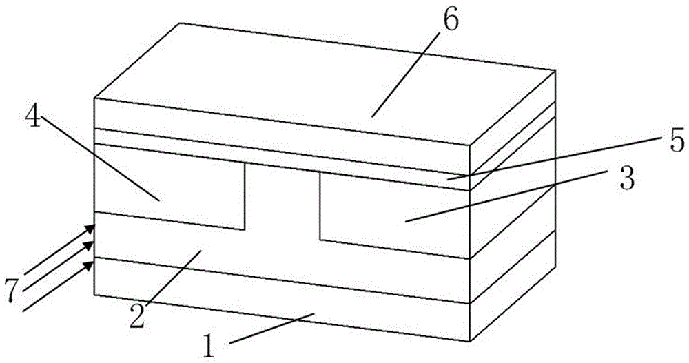
[0023] Example: Refer to figure 1 ,

[0024] A kind of SPP device device based on semiconductor gain and graphene, comprising sequentially stacked bottom graphene layer 1, semiconductor gain layer 2, buffer layer 5 and top layer graphene layer 6, and described semiconductor gain layer 2 is a T-shaped waveguide The two sides of the T-shaped waveguide structure are symmetrical first cuboid 3 and second cuboid 4 with the same structure and size.

[0025] The semiconductor gain layer 2 is an InGaAs layer with a high refractive index.

[0026] The first rectangular parallelepiped 3 and the second rectangular parallelepiped 4 are gallium arsenide with small dielectric constant and small electron effective mass, which can be used as epitaxial wafers.

[0027] The buffer layer 5 is a low refractive index cadmium sulfide buffer layer.

[0028] The frequency of SPPs generated at the bonding interface of two different layers can be controlled by adjusting the graphene thickness.

[0...


PUM


Abstract

The invention discloses an SPP device based on semiconductor gain and graphene, which is characterized by comprising a bottom-layer graphene layer, a semiconductor gain layer, a buffer layer and a top-layer graphene layer which are connected in a lapped manner in sequence, wherein the semiconductor gain layer is of a T-shaped waveguide structure, both sides of the T-shaped waveguide structure are provided with a first cuboid and a second cuboid which are symmetrical and of the same structure and size. The SPP device can provide stronger localized constraint, can provide a light source for a surface plasma excitation circuit, can be compatible with a variety of nano-photons and electronics devices, can provide a new prototype device for the development of high-density photonic integrated device such as a low-threshold nano laser, and can provide high-performance mcirocavities and an integratable device for the surface plasma field.

Description

technical field [0001] The invention relates to the technical field of optical communication, in particular to an SPP device based on semiconductor gain and graphene. Background technique [0002] Surface plasmon polaritons (SPP) is an electromagnetic mode between a light wave and a migratable surface charge realized by changing the subwavelength structure of the metal surface, which can support the surface plasmon wave transmitted at the interface between the metal and the medium. Light energy is thus transmitted without being limited by the diffraction limit. Because of this unique property of SPP, it plays an important role in manipulating light energy at the nanometer level. The ability of graphene to propagate spp properties has been theoretically demonstrated by an infinitely long graphene nanoribbon wrapped by quantum dots. "Optics Express" published a long article on pages 12925-12936 of Volume 19, Issue 14, 2011, which published a metal disc-shaped semiconductor r...

Claims


Application Information

Patent Timeline
Patent Type & Authority Applications(China)
IPC IPC(8): G02B5/00G02B6/122
CPCG02B5/008G02B6/1226
Inventor 秦柳丽朱君傅得立
Owner GUANGXI NORMAL UNIV
Why Eureka
Try Eureka