Discrete power mos field effect transistor and manufacturing method thereof

A technology of field effect tube and manufacturing method, which is applied in the field of discrete power mos field effect tube and its manufacturing, can solve the problems that P+ contact area cannot be formed, P+ injection cannot be formed, and is not easy to form, so as to improve the avalanche breakdown tolerance, The effect of reducing parasitic P+ resistance and simplifying the manufacturing process

Pending Publication Date: 2017-03-22
西安锴威半导体有限公司
View PDF3 Cites 2 Cited by
  • Summary
  • Abstract
  • Description
  • Claims
  • Application Information

AI Technical Summary

Problems solved by technology

[0002] Traditional discrete power mosfet manufacturing methods usually include 7-layer lithography termination ring lithography, active area lithography, polysilicon lithography, N+ lithography, contact hole lithography, metal lithography and passivation layer lithography A total of 7 layers of lithography, and N+ lithography is needed to determine the N+ implantation area during N+ implantation, otherwise, the P+ area that should not be implanted will be implanted with N+, because usually the N+ concentration is much higher than the P+ concentration, which will lead to If the P+ implantation after contact hole photolithography cannot be formed, the P+ contact region cannot be formed, and the process is cumbersome and difficult to form, such as figure 1 shown

Method used


Image

  • Discrete power mos field effect transistor and manufacturing method thereof
  • Discrete power mos field effect transistor and manufacturing method thereof
  • Discrete power mos field effect transistor and manufacturing method thereof

Examples


Embodiment Construction

[0027] The present invention is described in further detail below in conjunction with accompanying drawing:

[0028] A method for manufacturing a discrete power MOS field effect transistor, specifically comprising the following steps:

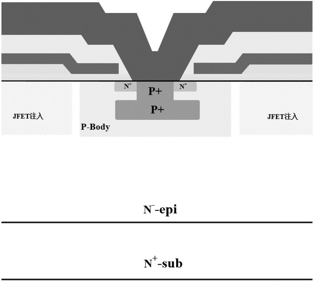
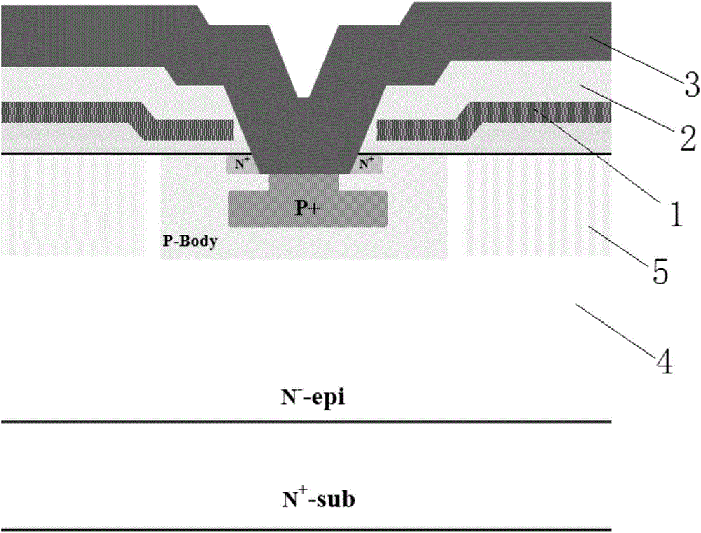
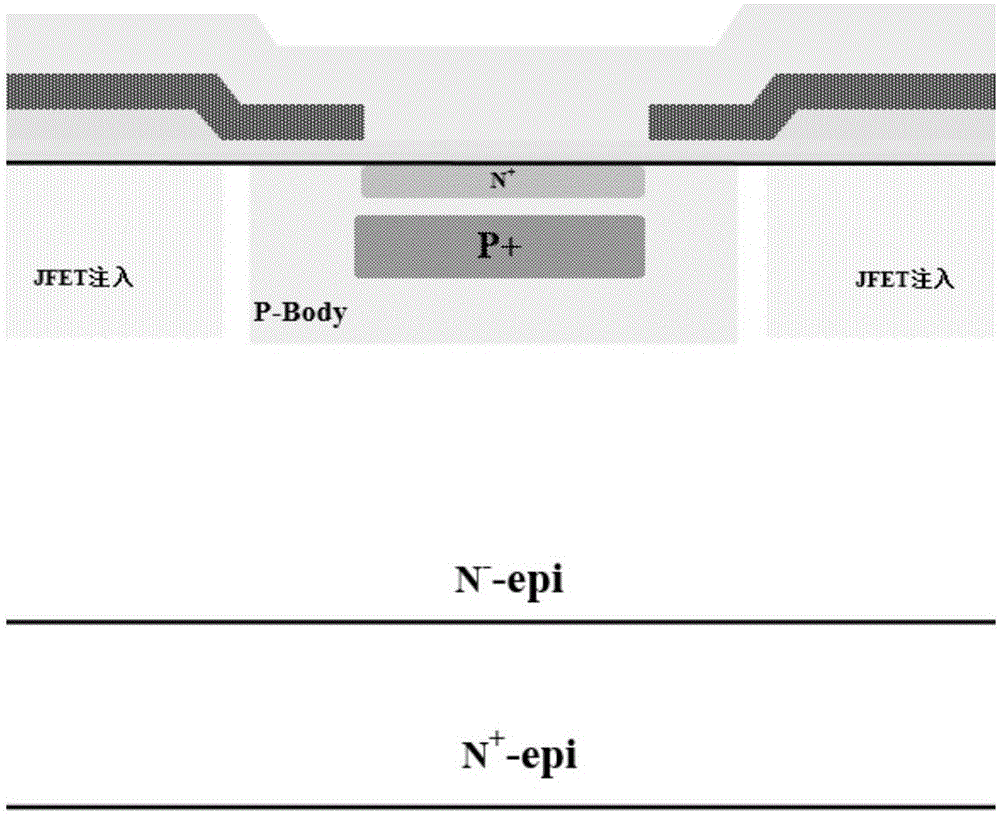
[0029] Step 1), first oxidizing the outer side of the epitaxial layer of the substrate, and then performing a terminal process to form a terminal;

[0030] Specifically, the outer side of the epitaxial layer of the substrate is oxidized, and then the terminal ring is sequentially subjected to photolithography, terminal ring implantation, terminal ring advancement, and field oxidation to form a terminal;

[0031] Wherein the substrate is an N-type substrate;

[0032] Step 2), then forming a source region in the epitaxial layer;

[0033] In the epitaxial layer where the source region needs to be formed, the photolithography of the active region is performed, and then the active region is etched, and then JFET implantation and gate oxide growth ...


PUM


Abstract

The invention discloses a discrete power mos field effect transistor and a manufacturing method thereof. In the process of forming the power mos field effect transistor, a source region is firstly formed in an epitaxial layer, contact hole corrosion is carried out on the formed source region, P+ injection and original P+ region connection are carried out on a contact hole region to form a P+ region, metal deposition is carried out to form a metal layer and contact of the metal layer and N+ and P+ of the source region is finally obtained. In the technical process, the lithography process of separately forming N+ and P+ through twice lithography corrosion in the original technical process is reduced, so that one-time lithography is reduced from the manufacturing process of a power MOS, and the manufacturing process is simplified and the production cost is reduced; a contact path of the P+ and the metal layer is shortened by adopting a silicon etching technology, so that parasitic P+ resistance is reduced to inhibit starting of a parasitic NPN and improvement of the avalanche breakdown tolerance is facilitated; and the source region is firstly formed and then contact hole corrosion is carried out on the formed source region, so that the trouble that P+ injection cannot be carried out after contact hole lithography due to the fact that the concentration of the N+ is much greater than that of the P+ is avoided.

Description

technical field [0001] The invention relates to a semiconductor power device, in particular to a discrete power mos field effect transistor and a manufacturing method thereof. Background technique [0002] Traditional discrete power mosfet manufacturing methods usually include 7-layer lithography termination ring lithography, active area lithography, polysilicon lithography, N+ lithography, contact hole lithography, metal lithography and passivation layer lithography A total of 7 layers of lithography, and N+ lithography is needed to determine the N+ implantation area during N+ implantation, otherwise, the P+ area that should not be implanted will be implanted with N+, because usually the N+ concentration is much higher than the P+ concentration, which will lead to If the P+ implantation after contact hole photolithography cannot be formed, the P+ contact region cannot be formed, and the process is cumbersome and difficult to form, such as figure 1 shown. The complexity an...

Claims


Application Information

Patent Timeline
Patent Type & Authority Applications(China)
IPC IPC(8): H01L29/78H01L29/08H01L21/336
CPCH01L29/0847H01L29/66477H01L29/78
Inventor 谭在超罗寅丁国华邹望杰
Owner 西安锴威半导体有限公司
Why Eureka
Try Eureka