
A LED epitaxial structure with stress compensation effect barrier layer

A technology of stress compensation and epitaxial structure, applied in the direction of semiconductor devices, electrical components, circuits, etc., can solve the problems of high background concentration, lower electromotive injection efficiency, lower recombination efficiency, etc., to increase the barrier height, improve internal quantum efficiency, The effect of improving compound efficiency

Active Publication Date: 2019-07-16
NANTONG TONGFANG SEMICON +1
View PDF4 Cites 0 Cited by
  • Summary
  • Abstract
  • Description
  • Claims
  • Application Information

AI Technical Summary

Problems solved by technology

In the traditional blue-light GaN-based LED epitaxial structure, due to the high background concentration of the GaN material, a large number of electrons overflow the quantum well into the P-type conductive layer, reducing the electrokinetic injection efficiency
At the same time, due to the limitation of electrons by the electron blocking layer, it also inhibits the injection of electromotive force and reduces the recombination efficiency.

Method used


Image

  • A LED epitaxial structure with stress compensation effect barrier layer
  • A LED epitaxial structure with stress compensation effect barrier layer
  • A LED epitaxial structure with stress compensation effect barrier layer

Examples


preparation example Construction

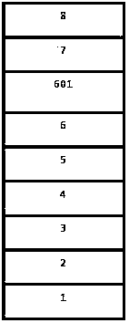
[0019] The preparation method of the structure of the present invention is to perform high-temperature baking in an MOCVD reaction furnace to remove residual impurities on the surface of the patterned substrate 1 , and slowly lower the temperature between 500-900° C. to grow a layer of AlN buffer layer 2 . Then the temperature is raised rapidly, and the U-shaped GaN layer 3 is grown at 900-1200° C. for about 10-80 minutes, with a thickness of 1-10 um. After that, the N-type GaN layer 4 is grown at a growth temperature of 800-1200° C., a growth time of 10-80 min, and a total growth thickness of 10-10000 nm. The shallow quantum well 5 is grown at a growth temperature of 680-880° C. and a total growth thickness of 10 nm-2000 nm. The active region 6 is grown at a growth temperature of 680-880°C, with a total growth thickness of 10nm-2000nm. A stress compensation layer 601 is grown. The electron blocking layer 7 is grown at 800-1000° C. with a thickness of 50-1000 angstroms. Re-...

Embodiment 1

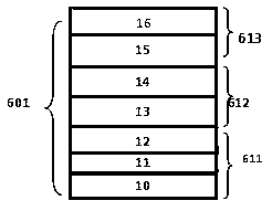
[0022] ① First grow the U-GaN layer 10, the growth temperature is 700°C, the growth pressure is 200mbar,

[0023] The growth thickness is 1nm; the growth temperature of U-AlGaN layer 11 is 700°C, the growth pressure is 200mbar, the growth thickness is 1nm, and the Al composition is 0.1; the growth temperature of U-InGaN layer 12 is 700°C, the growth pressure is 200mbar, and the growth thickness is 1nm, In composition 0.02.

[0024] ②Secondly, grow the N-AlGaN layer 13 at a growth temperature of 700°C, a growth pressure of 200mbar, a growth thickness of 1nm, an Al composition of 0.1, and a Si doping concentration of 5×10 17 ; The growth temperature of N-InGaN layer 14 is 700°C, the growth pressure is 200mbar, the growth thickness is 1nm, the In composition is 0.02, and the Si doping concentration is 5×10 17 .

[0025] ②Finally, grow the P-AlGaN layer 15 at a growth temperature of 700°C and a growth pressure of

[0026] 200mbar, the growth thickness is 1nm, the Al component i...

Embodiment 2

[0028] ① First grow the U-GaN layer 10 at a growth temperature of 800°C and a growth pressure of 400mbar,

[0029] The growth thickness is 1nm; the growth temperature of U-AlGaN layer 11 is 800°C, the growth pressure is 400mbar, the growth thickness is 1nm, and the Al composition is 0.2; the growth temperature of U-InGaN layer 12 is 800°C, the growth pressure is 400mbar, and the growth thickness is 1nm, and the In composition is 0.05 .

[0030] ③Secondly, the growth temperature of the N-AlGaN layer 13 is 800°C, and the growth pressure is

[0031] 400mbar, the growth thickness is 1nm, the Al composition is 0.2, and the Si doping concentration is 5×10 17 ; The growth temperature of N-InGaN layer 14 is 800°C, the growth pressure is 400mbar, the growth thickness is 1nm, the In composition is 0.05, and the Si doping concentration is 1×10 18 .

[0032] ④Finally, grow the P-AlGaN layer 15 at a growth temperature of 800°C and a growth pressure of

[0033] 400mbar, the growth thick...


PUM


Abstract

The invention relates to an LED epitaxial structure with a stress compensation effect barrier layer and belongs to the light emitting diode field. The LED epitaxial structure of the present invention comprises a patterned substrate, an AlN buffer layer, a U-type GaN layer, an N-type GaN layer, a shallow quantum well layer, an active region, an electron blocking layer and a P-type GaN layer which are distributed sequentially from bottom to top. The LED epitaxial structure is characterized in that the stress compensation effect barrier layer is arranged between the active region and the electron blocking layer; and the stress compensation effect barrier layer includes an intrinsic semiconductor layer, an N-type semiconductor layer and a P-type semiconductor layer which are distributed sequentially from bottom to top. According to the LED epitaxial structure of the invention, the barrier layer is additionally adopted, and therefore, electronic blocking efficiency can be improved, electric injection can be increased, efficiency decay can be decreased, and as a result, radiation recombination probability can be improved, and quantum efficiency in an LED can be improved.

Description

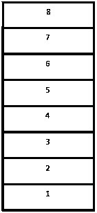
technical field [0001] The invention relates to the technical field of light-emitting diodes, in particular to LED epitaxy structures with stress compensation effect barrier layers. Background technique [0002] As blue GaN-based LEDs are more and more widely used, people pay more attention to the brightness of blue GaN-based LEDs. [0003] The blue-light GaN-based LED epitaxial structure in the prior art is as figure 1 As shown, from bottom to top are: patterned substrate 1, AlN buffer layer 2, U-type GaN layer 3, N-type GaN layer 4, shallow quantum well layer 5, active layer 6, electron blocking layer 7, P type GaN layer 8 . Due to the high background concentration of the GaN material in the traditional blue-light GaN-based LED epitaxial structure, a large number of electrons overflow the quantum well and enter the P-type conductive layer, reducing the electrokinetic injection efficiency. At the same time, due to the limitation of electrons by the electron blocking laye...

Claims


Application Information

Patent Timeline
Patent Type & Authority Patents(China)
IPC IPC(8): H01L33/12H01L33/06H01L33/14
CPCH01L33/06H01L33/12H01L33/14H01L33/145
Inventor 田宇郑建钦吴真龙曾颀尧董发李鹏飞
Owner NANTONG TONGFANG SEMICON
Learn More