Antimony-germanium multilayer nano-composite phase-change material and preparation and application thereof

A composite phase-change material and nano-composite technology, which is applied in antimony-germanium multilayer nano-composite phase-change materials and its preparation and application fields, can solve problems such as large RESET current, unfavorable data stability, and low crystal resistivity, and achieve Fast crystallization rate, slow change in crystallinity, low melting point effect

Inactive Publication Date: 2017-04-26
TONGJI UNIV
View PDF6 Cites 8 Cited by
  • Summary
  • Abstract
  • Description
  • Claims
  • Application Information

AI Technical Summary

Problems solved by technology

But its lower crystallization temperature is very unfavorable to the stability of data in PCRAM, and the crystalline resistivity of this material is lower simultaneously, needs bigger RESET electric current (G.Wang, X.Shen et al, AppliedPhysics Letters 103 (2013)031914)

Method used


Image

  • Antimony-germanium multilayer nano-composite phase-change material and preparation and application thereof
  • Antimony-germanium multilayer nano-composite phase-change material and preparation and application thereof
  • Antimony-germanium multilayer nano-composite phase-change material and preparation and application thereof

Examples


Embodiment 1

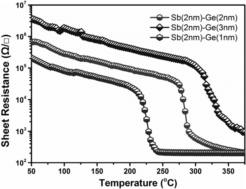
[0042] The total thickness of the Sb / Ge nanocomposite multilayer phase change film prepared in this example is 48-52nm, the general structure formula is [Sb(a)Ge(b)]x, and the specific structure has [Sb(2nm)Ge(1nm )] 16, [Sb(2nm)Ge(2nm)] 13, [Sb(2nm)Ge(3nm)] 10.

[0043] 1. Clean SiO2 2 / / Si(100) substrate surface and back, remove dust particles, organic and inorganic impurities:

[0044] (a) Place the substrate in an ethanol solution, and clean it ultrasonically for 15 minutes to remove dust particles and inorganic impurities on the surface of the substrate;

[0045] (b) The substrate is placed in an acetone solution, and ultrasonically cleaned for 15 minutes to remove organic impurities on the surface of the substrate;

[0046] (c) Place the substrate in deionized water, clean it ultrasonically for 15 minutes, and clean the surface again;

[0047] (d) Take out the substrate, dry it with pure Ar gas, and set it aside.

[0048] 2. Preparation of [Sb(a)Ge(b)]x films by sputte...

Embodiment 2

[0058] The total thickness of the Sb / Ge nanocomposite multilayer phase change film prepared in this example is 48nm, and the specific structure is [Sb(2nm)Ge(1nm)]16.

[0059] 1. Clean SiO2 2 / Si(100) substrate surface and back, remove dust particles, organic and inorganic impurities:

[0060] (a) Place the substrate in an ethanol solution, and clean it ultrasonically for 15 minutes to remove dust particles and inorganic impurities on the surface of the substrate;

[0061] (b) The substrate is placed in an acetone solution, and ultrasonically cleaned for 15 minutes to remove organic impurities on the surface of the substrate;

[0062] (c) Place the substrate in deionized water, clean it ultrasonically for 15 minutes, and clean the surface again;

[0063] (d) Take out the substrate, dry it with pure Ar gas, and set it aside.

[0064] 2. Preparation of [Sb(2nm)Ge(1nm)]16 film by sputtering method

[0065] (a) Put the Sb and Ge alloy targets, install the substrate, and then s...

Embodiment 3

[0074] The total thickness of the Sb / Ge nanocomposite multilayer phase change film prepared in this example is 52nm, and the specific structure is [Sb(2nm)Ge(2nm)]13.

[0075] 1. Clean SiO2 2 / Si(100) substrate surface and back, remove dust particles, organic and inorganic impurities:

[0076] (a) Place the substrate in an ethanol solution, and clean it ultrasonically for 15 minutes to remove dust particles and inorganic impurities on the surface of the substrate;

[0077] (b) The substrate is placed in an acetone solution, and ultrasonically cleaned for 15 minutes to remove organic impurities on the surface of the substrate;

[0078] (c) Place the substrate in deionized water, clean it ultrasonically for 15 minutes, and clean the surface again;

[0079] (d) Take out the substrate, dry it with pure Ar gas, and set it aside.

[0080] 2. Preparation of [Sb(2nm)Ge(2nm)]13 film by sputtering method

[0081] (a) Put Sb and Ge single target materials, install the substrate, and ...


PUM

PropertyMeasurementUnit
thicknessaaaaaaaaaa
thicknessaaaaaaaaaa
thicknessaaaaaaaaaa

Abstract

The invention relates to an antimony-germanium multilayer nano-composite phase-change material and preparation and application thereof. The composite phase-change material comprises a multilayer film structure formed by alternative arrangement of Sb films and Ge films, the thickness of the Sb film is 1-3 nm, and the thickness of the Ge film is 0.5-3.5 nm. By employing a magnetron sputtering method, multiple layers of Sb films and Ge films are alternatively deposited on a SiO2/Si (100) substrate by regarding Sb and Ge as sputtering target materials and regarding Ar as the sputtering gas, and the Sb/Ge nano-composite multilayer phase-change film material is obtained. Compared with the prior art, according to the Sb/Ge nano-composite multilayer phase-change film, the thermal stability is high, and the saving time of data can be increased; crystalline and amorphous resistances are higher, and the operation power consumption of a PCRAM can be reduced; and compared with the conventional phase-change storage material, the thermal stability is improved, and the crystallization speed is accelerated.

Description

technical field [0001] The invention relates to the technical field of microelectronics, in particular to an antimony-germanium multilayer nanocomposite phase-change material and its preparation and application. Background technique [0002] Since the beginning of the 21st century, information has shown explosive growth in mass, digitization and networking, and the level of informatization has become an important symbol to measure the level of modernization and development of a country or region. Informatization is the core driving force to promote urbanization and industrialization, and integrated circuit chips are the cornerstone of informatization. In recent years, the market share of semiconductor memory has increased year by year, and has already occupied about a quarter of the entire integrated circuit. Phase change memory (Phase Change Random Access Memory, abbreviated as PCRAM). Among various new memories, it has been recognized as one of the most promising memorie...

Claims


Application Information

Patent Timeline
Patent Type & Authority Applications(China)
IPC IPC(8): H01L45/00B82Y30/00
CPCB82Y30/00H10N70/881H10N70/026
Inventor 翟继卫陈施谕吴卫华
Owner TONGJI UNIV
Why Eureka
Try Eureka