Semiconductor device and preparation method thereof, and electronic apparatus

A semiconductor and device technology, applied in the field of semiconductor devices and their preparation, can solve problems affecting device performance, spacer failure, spacer damage, etc.

Active Publication Date: 2017-05-03
SEMICON MFG INT (SHANGHAI) CORP +1
View PDF4 Cites 3 Cited by
  • Summary
  • Abstract
  • Description
  • Claims
  • Application Information

AI Technical Summary

Problems solved by technology

[0004] For NOR flash memory, the threshold voltage should remain stable, and its threshold voltage depends on the electrons in the floating gate. Through gate disturbance testing, it is found that the threshold voltage stability of NOR flash memory becomes worse as the size of semiconductor devices continues to decrease. , the reason may be that the spacer on the gate is damaged when the contact hole opening is formed between the gates, which affects the performance of the device and even makes the spacer invalid

Method used


Image

  • Semiconductor device and preparation method thereof, and electronic apparatus
  • Semiconductor device and preparation method thereof, and electronic apparatus
  • Semiconductor device and preparation method thereof, and electronic apparatus

Examples


Embodiment 1

[0036] A specific embodiment of the present invention will be described below in conjunction with the accompanying drawings, wherein, Figures 1a-1e It is a schematic diagram of the preparation process of the semiconductor device described in one embodiment of the present invention; figure 2 It is a flow chart of the manufacturing process of the semiconductor device described in one embodiment of the present invention.

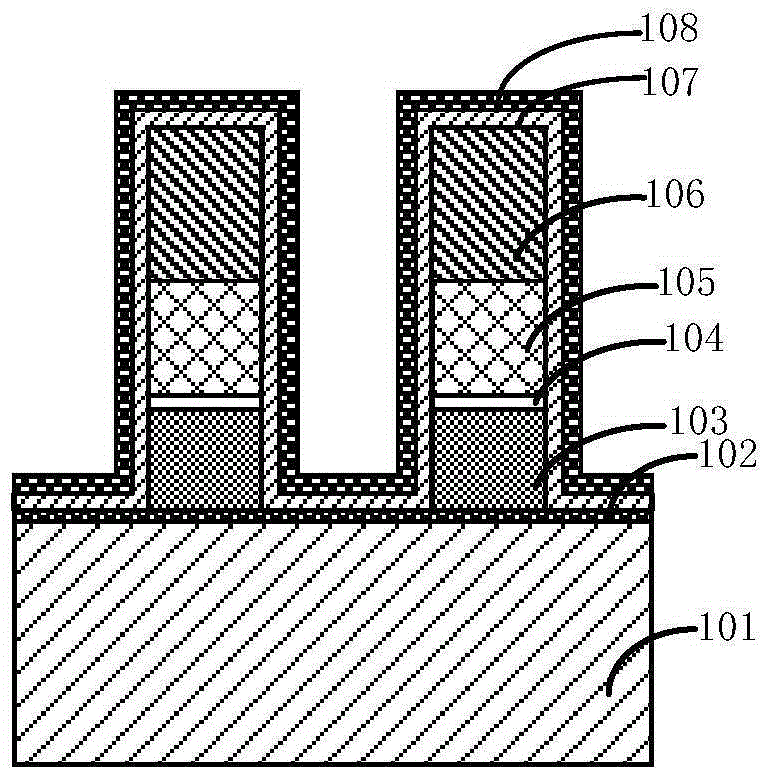
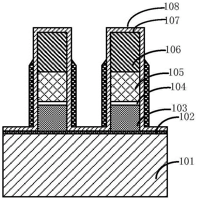
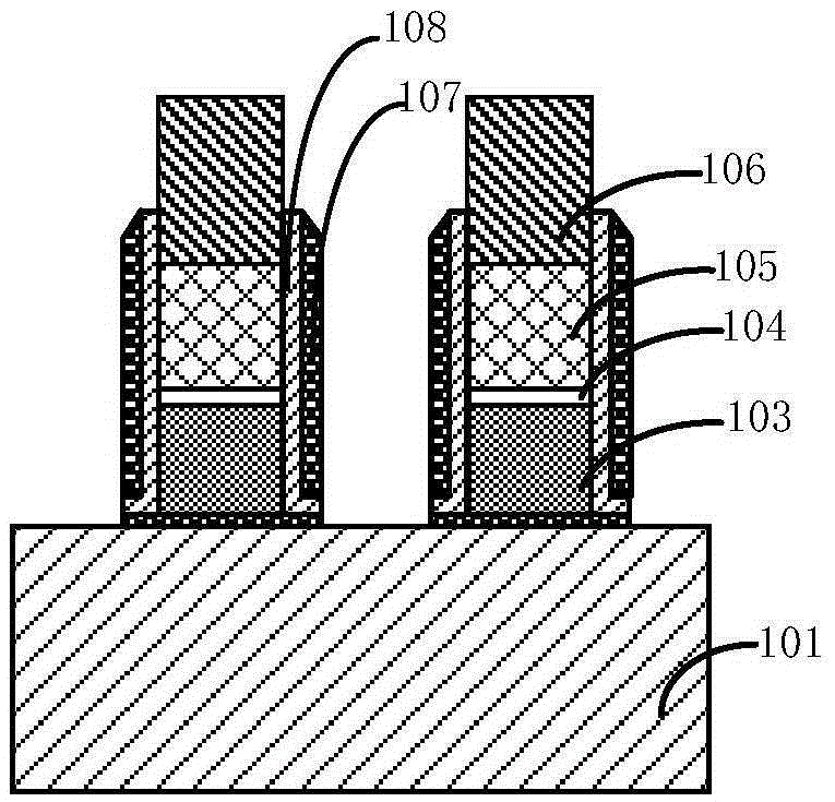
[0037] First, step 101 is performed to provide a semiconductor substrate 101 on which a gate dielectric layer is formed.

[0038] First, refer to Figure 1a , wherein the semiconductor substrate 101 can be at least one of the materials mentioned below: silicon, silicon-on-insulator (SOI), silicon-on-insulator (SSOI), silicon-germanium-on-insulator (S-SiGeOI) , silicon germanium on insulator (SiGeOI) and germanium on insulator (GeOI), etc.

[0039] In addition, an active region may be defined on the semiconductor substrate 101 . Other active devices may als...

Embodiment 2

[0089] The present invention also provides a semiconductor device, the semiconductor device includes a semiconductor substrate, the semiconductor substrate 101 can be at least one of the materials mentioned below: silicon, silicon-on-insulator (SOI), on-insulator Stacked silicon (SSOI), stacked silicon germanium on insulator (S-SiGeOI), silicon germanium on insulator (SiGeOI) and germanium on insulator (GeOI), etc.

[0090] In addition, an active region may be defined on the semiconductor substrate 101 . Other active devices may also be included on the active area, which are not marked in the shown figures for convenience.

[0091] A gate dielectric layer 102 is formed on the semiconductor substrate 101 , wherein the gate dielectric layer 102 may be a dielectric material commonly used in the field, for example, an oxide may be selected.

[0092] When oxide is selected as the gate dielectric layer 102 , the formation method of the gate dielectric layer 102 can be high temperat...

Embodiment 3

[0105] The present invention also provides an electronic device, including the semiconductor device described in the second embodiment. Wherein, the semiconductor device is the semiconductor device described in the second embodiment, or the semiconductor device obtained according to the preparation method described in the first embodiment.

[0106] The electronic device of this embodiment can be any electronic product or equipment such as mobile phone, tablet computer, notebook computer, netbook, game console, TV set, VCD, DVD, navigator, camera, video recorder, voice recorder, MP3, MP4, PSP, etc. , can also be any intermediate product including the semiconductor device. The electronic device according to the embodiment of the present invention has better performance due to the use of the above-mentioned semiconductor device.


PUM


Abstract

The invention relates to a semiconductor device and a preparation method thereof, and an electronic apparatus. The method comprises the following steps: S1, providing a semiconductor substrate, wherein a plurality of gate laminations are formed on the semiconductor substrate, and the gate laminations include a floating gate, an isolation layer, a control gate and a mask layer which are laminated in turn; S2, sequentially forming a first gap wall material layer and a second gap wall material layer on the semiconductor substrate and the gate laminations to cover the gate laminations, wherein the first gap wall material layer is made of oxide; S3, etching the second gap wall material layer to expose the first gap wall material layer on the semiconductor substrate and on the upper sidewall of the mark layer; S4, removing the exposed first gap wall material layer through etching to form a gap wall on the sidewall of the gate laminations; and S5, depositing a stop layer to cover the gap wall and the mask layer. Through the method, the yield and performance of NOR flash memories are improved.

Description

technical field [0001] The present invention relates to a semiconductor device, in particular, the present invention relates to a semiconductor device, a preparation method thereof, and an electronic device. Background technique [0002] With the rapid development of portable electronic devices (such as mobile phones, digital cameras, MP3 players, and PDAs, etc.), the requirements for data storage are getting higher and higher. Non-volatile flash memory has become the most important storage component in these devices due to its ability to save data even when power is off. Among them, because flash memory (flash memory) can achieve high chip storage density, and does not introduce new materials , The manufacturing process is compatible, therefore, it can be more easily and reliably integrated into own digital and analog circuits. [0003] NOR and NAND are two main non-volatile flash memory technologies on the market today. NOR flash memory (Flash) devices are a type of non-v...

Claims


Application Information

Patent Timeline
Patent Type & Authority Applications(China)
IPC IPC(8): H01L21/336H01L27/11517H01L27/11524
CPCH01L29/66833H10B43/30
Inventor 张翼英陈卓凡
Owner SEMICON MFG INT (SHANGHAI) CORP
Why Eureka
Try Eureka