Niobium-silicon-based glass energy storage material with high energy storage density and preparation and application thereof
A technology of high energy storage density and energy storage materials, which is applied in the field of dielectric energy storage materials, can solve problems such as breakdown reduction, and achieve the effects of excellent breakdown resistance, high energy storage density, and good machining performance
- Summary
- Abstract
- Description
- Claims
- Application Information
AI Technical Summary
Problems solved by technology
Method used
Image
Examples
Embodiment 1
[0033] (1) BaCO with a purity greater than 99.95wt% 3 , Nb 2 o 5 and SiO 2 For raw material batching, the molar percentages of the above components are 32%, 32% and 36%. After adding alcohol to moisten and ball mill the mixture for 24 hours, dry it, and melt it at 1520°C for 3 hours;
[0034] (2) The high-temperature melt obtained in step (1) is clarified at 1520° C. for 2 hours, poured into a metal mold, and annealed for stress relief at 600° C. for 5 hours to prepare a niobium-silicon-based glass-ceramic energy storage material with high energy storage density;
[0035] (3) Cutting the glass prepared in step (2) to obtain glass flakes with a thickness of 0.9 mm.
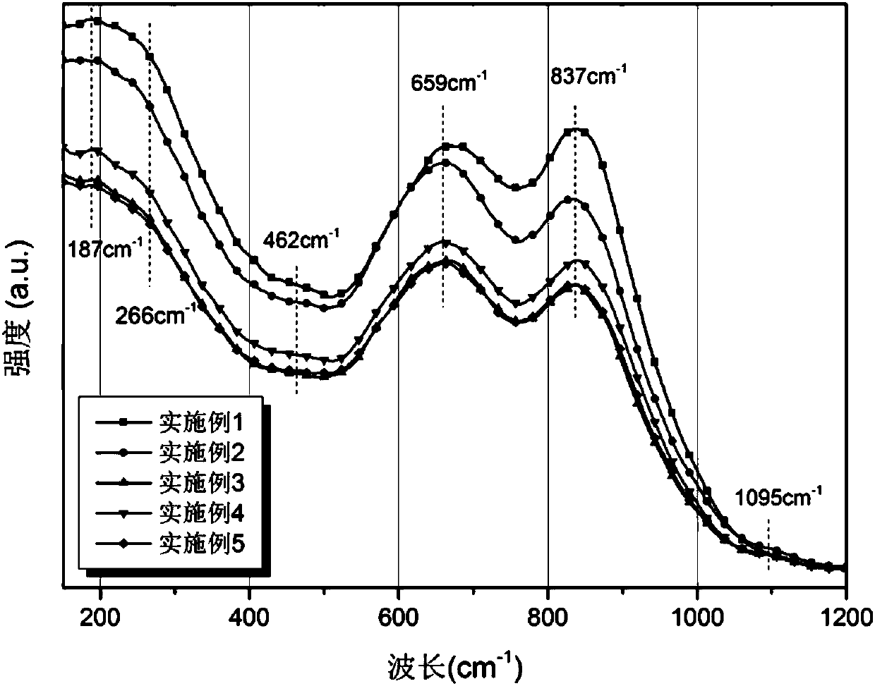
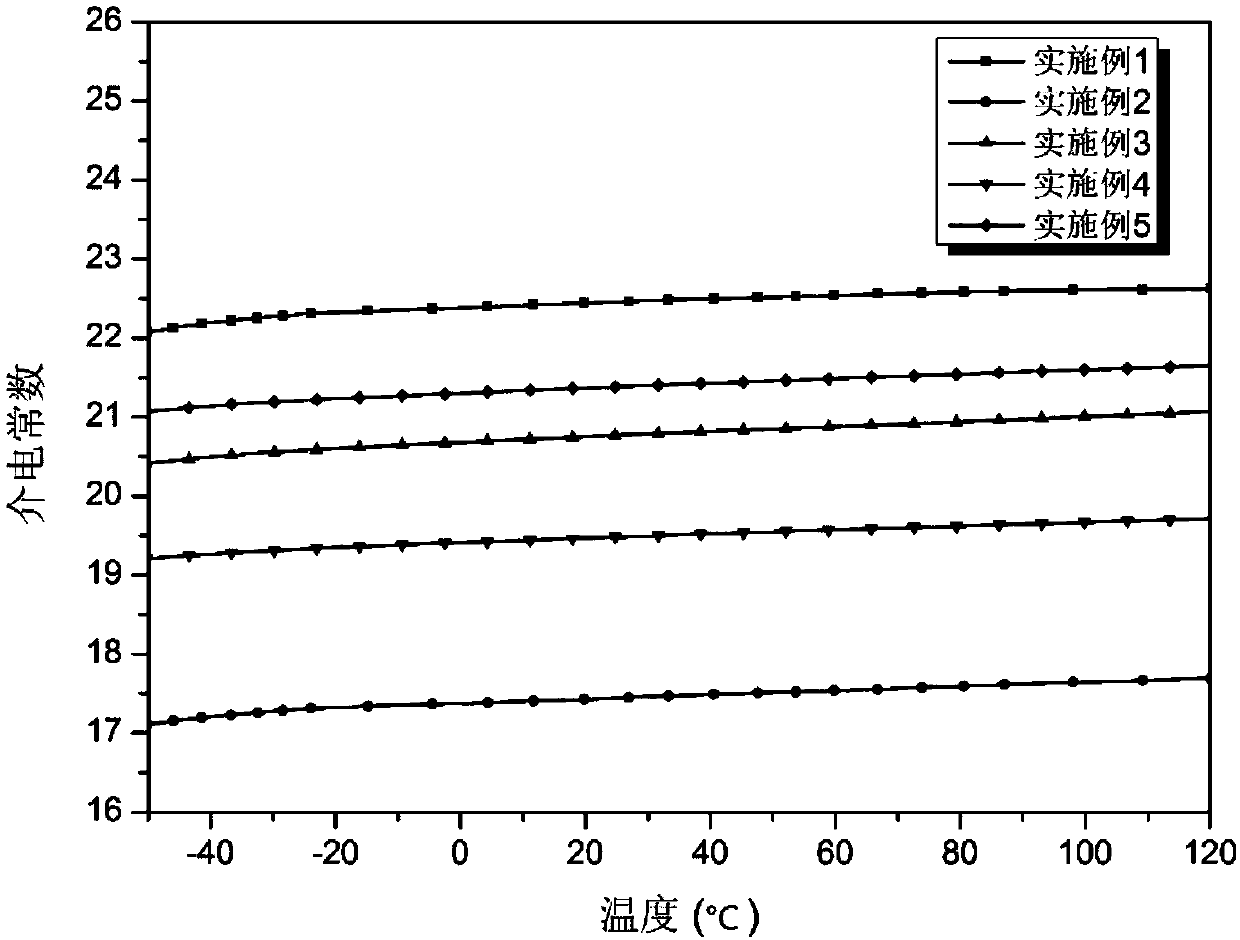
[0036] The Raman spectrum of the sample that present embodiment makes is as figure 2 As shown, the dielectric properties are as image 3 As shown, the withstand voltage performance test is as follows Figure 4 As shown, the energy storage density is shown in Table 1.
Embodiment 2
[0038] (1) BaCO with a purity greater than 99.95wt% 3 , Li 2 CO 3 , Nb 2 o 5 and SiO 2For raw material ingredients, the molar percentages of the above components are 25.6%, 6.4%, 32% and 36%. After ball milling for 24 hours, dry and melt at 1500°C for 3 hours;
[0039] (2) pour the high-temperature melt obtained in step (1) into a metal mold after being clarified at 1500°C for 2 hours, and then stress-relief annealed at 600°C for 5 hours to prepare a niobium-silicon-based glass-ceramic energy storage material with high energy storage density;
[0040] (3) Cutting the glass prepared in step (2) to obtain glass flakes with a thickness of 0.9 mm.
[0041] The Raman spectrum of the sample that present embodiment makes is as figure 2 As shown, the dielectric properties are as image 3 As shown, the withstand voltage performance test is as follows Figure 4 As shown, the energy storage density is shown in Table 1.
Embodiment 3
[0043] (1) BaCO with a purity greater than 99.95wt% 3 、Na 2 CO 3 , Nb 2 o 5 and SiO 2 For raw material ingredients, the molar percentages of the above components are 25.6%, 6.4%, 32% and 36%. After ball milling and mixing for 24 hours, dry and melt at 1520°C for 3 hours;
[0044] (2) The high-temperature melt obtained in step (1) is clarified at 1520° C. for 2 hours, poured into a metal mold, and annealed for stress relief at 600° C. for 5 hours to prepare a niobium-silicon-based glass-ceramic energy storage material with high energy storage density;
[0045] (3) Cutting the glass prepared in step (2) to obtain glass flakes with a thickness of 0.9 mm.
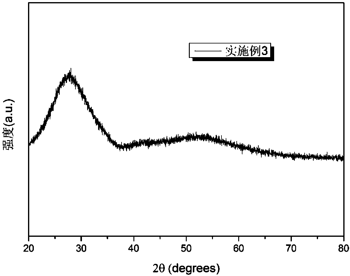
[0046] The XRD of the sample that present embodiment makes is as figure 1 As shown, the Raman spectrum is shown as figure 2 As shown, the dielectric properties are as image 3 As shown, the withstand voltage performance test is as follows Figure 4 As shown, the energy storage density is shown in Table 1.
PUM
| Property | Measurement | Unit |
|---|---|---|
| Thickness | aaaaa | aaaaa |
Abstract
Description
Claims
Application Information


