Adhesive tape for semiconductor wafer surface protection

A semiconductor and adhesive tape technology, which is applied in semiconductor/solid-state device manufacturing, film/flaky adhesives, adhesives, etc., can solve the problems of rough gold bumps, incompatibility, and deterioration of thickness accuracy, and achieve easy peeling Effect

Active Publication Date: 2020-01-07
FURUKAWA ELECTRIC CO LTD
View PDF12 Cites 0 Cited by
  • Summary
  • Abstract
  • Description
  • Claims
  • Application Information

AI Technical Summary

Problems solved by technology

[0011] However, since the surface of the gold bump is very rough in many cases, after the adhesive tape for protecting the surface of the pressure-sensitive semiconductor wafer is peeled off, the residue of the adhesive layer adheres to the surface of the gold bump. question
Therefore, if the adhesive residue is not allowed to occur, after the adhesive tape for protecting the semiconductor wafer surface is bonded to the semiconductor wafer, the adhesive tape for protecting the semiconductor wafer surface will float from the semiconductor wafer over time, When the thickness accuracy after grinding deteriorates or dust enters during grinding
Adhesion to gold bumps during grinding and peelability after grinding have a mutual compensation relationship, and it is impossible to balance both
[0012] For this problem, develop a kind of by adjusting the contact angle value etc. to diiodomethane to improve the adhesive tape for ultraviolet curable semiconductor wafer surface protection of releasability (refer for example patent document 4), or similarly borrow Pressure-sensitive adhesive tapes for protecting the surface of semiconductor wafers whose releasability is improved by adjusting the value of the contact angle to diiodomethane (see, for example, Patent Document 5), as long as these adhesive tapes for protecting the surface of semiconductor wafers are used, can solve the problem of residual glue on the active surface, but the adhesion and peelability of the gold bumps still cannot be satisfied at the same time.

Method used


Image

  • Adhesive tape for semiconductor wafer surface protection
  • Adhesive tape for semiconductor wafer surface protection
  • Adhesive tape for semiconductor wafer surface protection

Examples


Embodiment 1

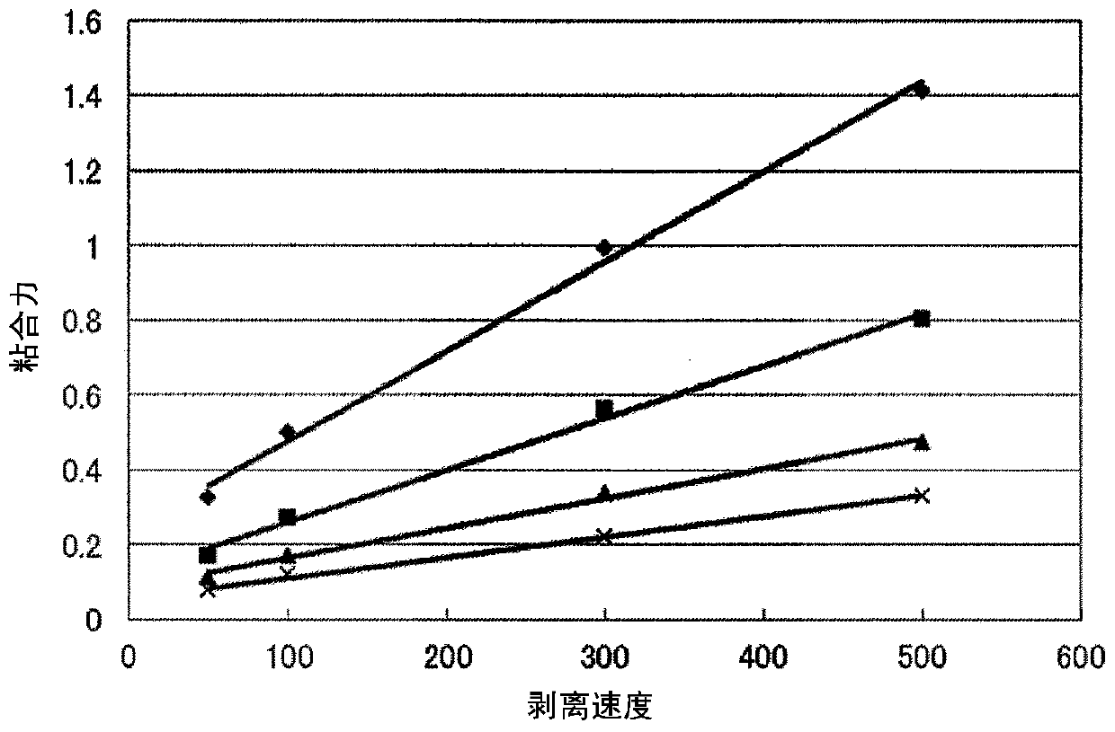
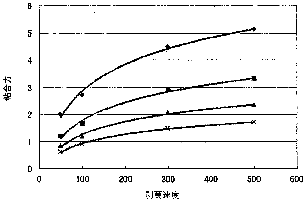
[0072] With respect to 100 parts by mass of an acrylic copolymer mainly composed of acrylic acid and 2-ethylhexyl acrylate, with an acid value of 57.8 mgKOH / g and a weight average molecular weight of 800,000, an epoxy curing agent TETRAD is blended as a crosslinking agent -X (manufactured by Mitsubishi Gas Chemical Co., Ltd.) was 0.5 parts by mass to obtain a solvent-based adhesive composition. Coating the adhesive composition on a polyethylene terephthalate (PET) spacer with a thickness of 38 μm so that the film thickness after drying becomes 50 μm, and after drying, sticking to the ethylene-vinyl acetate spacer with a thickness of 120 μm An ester copolymer (EVA) film was laminated to produce the adhesive tape for protecting the surface of a semiconductor wafer related to Example 1.

Embodiment 2

[0074] With respect to 100 parts by mass of an acrylic copolymer containing acrylic acid and 2-ethylhexyl acrylate as main components, an acid value of 23.2 mgKOH / g, and a weight average molecular weight of 700,000, an epoxy curing agent as a crosslinking agent is mixed 0.5 parts by mass of TETRAD-X (manufactured by Mitsubishi Gas Chemical Co., Ltd.) was used to obtain a solvent-based adhesive composition. Coating the adhesive composition on a polyethylene terephthalate (PET) spacer with a thickness of 38 μm so that the film thickness after drying becomes 50 μm, and after drying, sticking to the ethylene-vinyl acetate spacer with a thickness of 120 μm An ester copolymer (EVA) film was laminated to produce an adhesive tape for protecting the surface of a semiconductor wafer related to Example 2.

Embodiment 3

[0076] With respect to 100 parts by mass of an acrylic copolymer mainly composed of acrylic acid and 2-ethylhexyl acrylate, with an acid value of 46.6 mgKOH / g and a weight average molecular weight of 900,000, an epoxy curing agent is blended as a crosslinking agent 0.5 parts by mass of TETRAD-X (manufactured by Mitsubishi Gas Chemical Co., Ltd.) was used to obtain a solvent-based adhesive composition. Coating the adhesive composition on a polyethylene terephthalate (PET) spacer with a thickness of 38 μm so that the film thickness after drying becomes 50 μm, and after drying, sticking to the ethylene-vinyl acetate spacer with a thickness of 120 μm An ester copolymer (EVA) film was laminated to produce an adhesive tape for protecting the surface of a semiconductor wafer related to Example 3.


PUM

PropertyMeasurementUnit
acid valueaaaaaaaaaa
thicknessaaaaaaaaaa
thicknessaaaaaaaaaa

Abstract

The object of the present invention is to provide an adhesive tape for protecting the surface of a semiconductor wafer, which does not cause floating phenomenon even if it is attached to a semiconductor wafer having gold bumps and placed, and is suitable for polishing the back surface of a semiconductor wafer. During this time, dust or water will not be immersed, and the semiconductor wafer can be ground into a film, and the semiconductor wafer can be peeled off without cracking or residual glue. The means for solving the problem is an adhesive tape for protecting the surface of a semiconductor wafer, which has at least an adhesive layer and a base film, and the adhesive layer is not cured by the irradiation of energy rays, and the peeling speed is reduced at 23°C. The ratio B / A of the adhesive force A of the SUS280 abrasive surface at 50mm / min to the adhesive force B of the SUS280 abrasive surface at a peeling speed of 500mm / min is lower than 4.0, and for the SUS280 abrasive surface at a peeling speed of 300mm / min The adhesive force is 1.2-4.5N / 25mm at 23°C, and the adhesive force at 50°C is less than 50% of the adhesive force at 23°C.

Description

technical field [0001] The invention relates to an adhesive tape for protecting the surface of a semiconductor wafer. More specifically, it relates to an adhesive tape for semiconductor wafer surface protection used when polishing a semiconductor wafer into a thin film. Background technique [0002] Semiconductor packaging is manufactured by cutting high-purity monocrystalline silicon into semiconductor wafers, and then forming integrated circuits on the surface of the wafers by ion implantation and etching. The back surface of the semiconductor wafer on which the integrated circuit is formed is ground, and the semiconductor wafer is made into a desired thickness by grinding or other methods. At this time, in order to protect the integrated circuits formed on the surface of the semiconductor wafer, an adhesive tape for protecting the surface of the semiconductor wafer can be used. After the back grinding, the semiconductor wafers will be stored in the wafer box after the b...

Claims


Application Information

Patent Timeline
Patent Type & Authority Patents(China)
IPC IPC(8): H01L21/304C09J7/20
CPCH01L21/304C09J7/20
Inventor 横井启时
Owner FURUKAWA ELECTRIC CO LTD
Why Eureka
Try Eureka