Manufacturing method of high-speed PCB and PCB

A manufacturing method and high-speed technology, which can be used in multilayer circuit manufacturing, printed circuit manufacturing, and electrical connection formation of printed components, etc. Effect

A manufacturing method and high-speed technology, which can be used in multilayer circuit manufacturing, printed circuit manufacturing, and electrical connection formation of printed components, etc. Effect

CN106793577AActive Publication Date: 2017-05-31DONGGUAN SHENGYI ELECTRONICS

Image

  • Manufacturing method of high-speed PCB and PCB
  • Manufacturing method of high-speed PCB and PCB
  • Manufacturing method of high-speed PCB and PCB

Examples


Embodiment Construction

[0041] In order to elaborate the technical solutions adopted by the present invention to achieve the predetermined technical purpose, the technical solutions in the embodiments of the present invention will be clearly and completely described below with reference to the accompanying drawings in the embodiments of the present invention. Obviously, the described implementation The examples are only some of the embodiments of the present invention, not all of the embodiments, and the technical means or technical features in the embodiments of the present invention can be replaced without creative work. The following will refer to the accompanying drawings in conjunction with Examples are given to illustrate the present invention in detail.

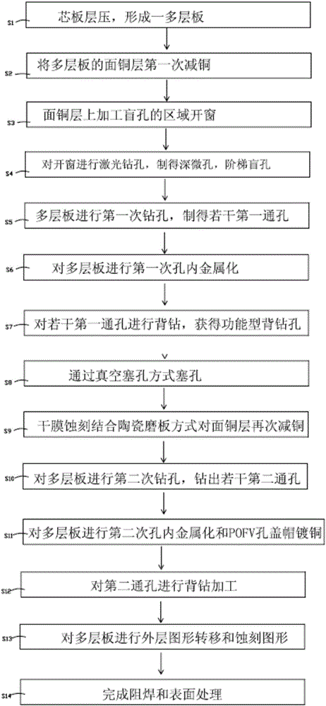
[0042] see figure 1 , a high-speed PCB production method, using a new process route to achieve high-speed PCB production. The specific production steps are as follows:

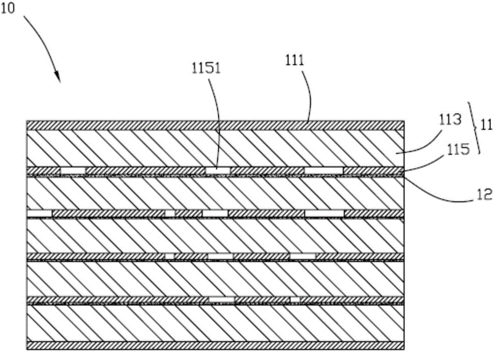
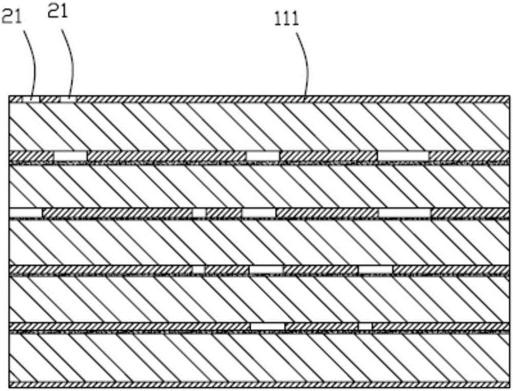
[0043] 1) Several core boards are laminated after the inner layer patt...


PUM

PropertyMeasurementUnit
thicknessaaaaaaaaaa

Abstract

The invention provides a manufacturing method of a high-speed PCB and the PCB. The manufacturing method includes the following steps that 1, lamination is carried out after a normal inner layer graph is manufactured; 2, copper reduction is carried out to achieve the size of 6 micrometers to 8 micrometers after lamination is completed; 3, +4.5 mil copper etching windowing is carried out on a deep micropore region and a first-order blind hole region overall; 4, laser drilling is carried out to complete deep micropore and first-order blind hole machining; 5, through holes needing resin hole plugging are mechanically drilled for the first time; 6, the interiors of the holes are metalized for the first time; 7, the through holes are back-drilled for the first time; 8, vacuum hole plugging is carried out; 9, the holes are covered with dry films, single side +5 mil dry film covering is carried out on deep micropores, first-order blind holes and the first through holes; 10, chemical copper reduction and ceramic grinding plate copper reduction are carried out to achieve the size of 20 micrometers to 25 micrometers; 11, second through holes are mechanically drilled; 12, the interiors of the holes are metalized for the second time, and POFV blocking is carried out; 13, the second through holes are back-drilled, and connection type functional holes are machined; 14, an outer layer graph is transferred, and a fine line graph is etched; 15, solder resisting and surface treatment are completed. The high-complexity high-speed PCB can be manufactured, the manufacturing period is short, and the cost is low.

Description

technical field [0001] The invention relates to a manufacturing method of a circuit board, in particular to a manufacturing method of a high-speed PCB and the PCB. Background technique [0002] With the rapid development of high-density integrated circuit technology and microelectronics technology, the volume of electronic products has become lighter, thinner and smaller, with highly dense functions and stronger performance. At present, in order to meet the high-speed and high-density requirements of products, the PCB design combines deep micro-holes, blind holes, back drilling, POFV (Plating Over Filled Via, need to plug holes), dense lines and other processes together. High aspect ratio through blind hole electroplating process capability, high aspect ratio through, blind hole, back drilling, resin plug hole control, circuit accuracy control ability, surface treatment compatibility, etc. all pose great challenges. The existing conventional Equipment and process methods ar...

Claims


Application Information

Patent Timeline
31 May 2017
Publication
CN106793577A
IPC
H05K3/42; H05K3/46
CPC
H05K3/429; H05K3/46; H05K2201/096; H05K2203/0214
Inventors
王小平; 杜红兵