Process for producing layer of organic perovskite material with improved crystallinity

一种晶体材料、有机阴离子的技术,应用在铜有机化合物、锡有机化合物、铅有机化合物等方向,能够解决没有很好地理解钙钛矿等问题,达到膜光滑度改善的效果

Active Publication Date: 2017-05-31
OXFORD UNIV INNOVATION LTD
View PDF2 Cites 16 Cited by
  • Summary
  • Abstract
  • Description
  • Claims
  • Application Information

AI Technical Summary

Problems solved by technology

Although the device performance of perovskite solar cells has improved at an unprecedented rate in recent years, organic-inorganic metal halide perovskites (e.g., CH 3 NH 3 wxya 3 , where X = Cl, Br, I, also referred to herein as MAPbX 3 ), such as the role of cations and anions

Method used


Image

  • Process for producing layer of organic perovskite material with improved crystallinity
  • Process for producing layer of organic perovskite material with improved crystallinity
  • Process for producing layer of organic perovskite material with improved crystallinity

Examples


Embodiment 1

[0324] Example 1: Sacrificial anion

[0325] method

[0326] Preparation of Perovskite Precursors

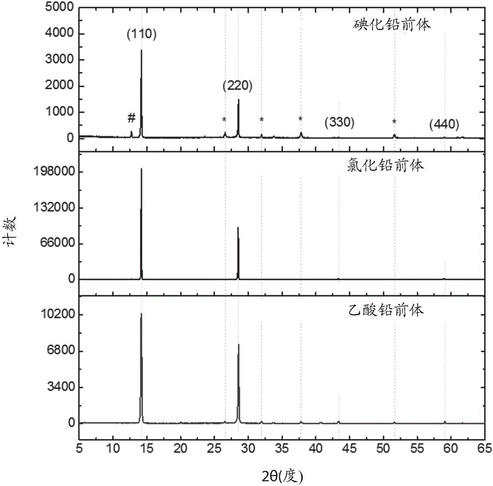
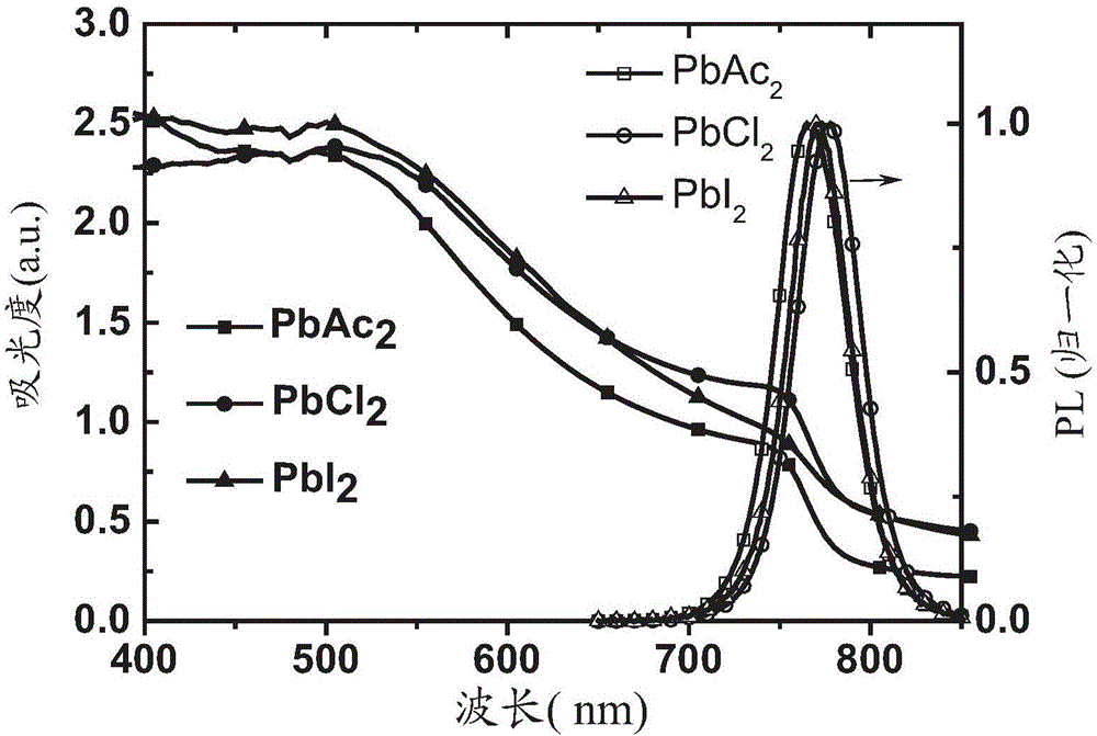
[0327] Methylammonium iodide (MAI) was prepared by reacting 33 wt% methylamine (Sigma-Aldrich) in ethanol with 57 wt% hydroiodic acid (HI) in water (Sigma-Aldrich) at room temperature. HI was added dropwise with stirring. Upon drying at 100 °C, a white powder formed, which was dried in a vacuum oven overnight and purified with ethanol before use. To form a perovskite precursor solution, MAI and PbX 2 (X=Ac, Cl, I, wherein Ac is the acetate ion H 3 CCOO – ) was dissolved in anhydrous N,N-dimethylformamide (DMF) at a molar ratio of 3:1 to a final perovskite precursor concentration of ~40 wt%.

[0328] Substrate preparation

[0329] The glass substrates for photoluminescence (PL) measurement were sequentially cleaned with 2% hallmanex detergent, acetone, 2-propanol and oxygen plasma. Fluorine-doped tin oxide (FTO) coated glass (Pilkington, 7Ω□ -1 ) to fabricate devices. T...

Embodiment 2

[0374] Example 2: Sacrificial anions and sacrificial cations

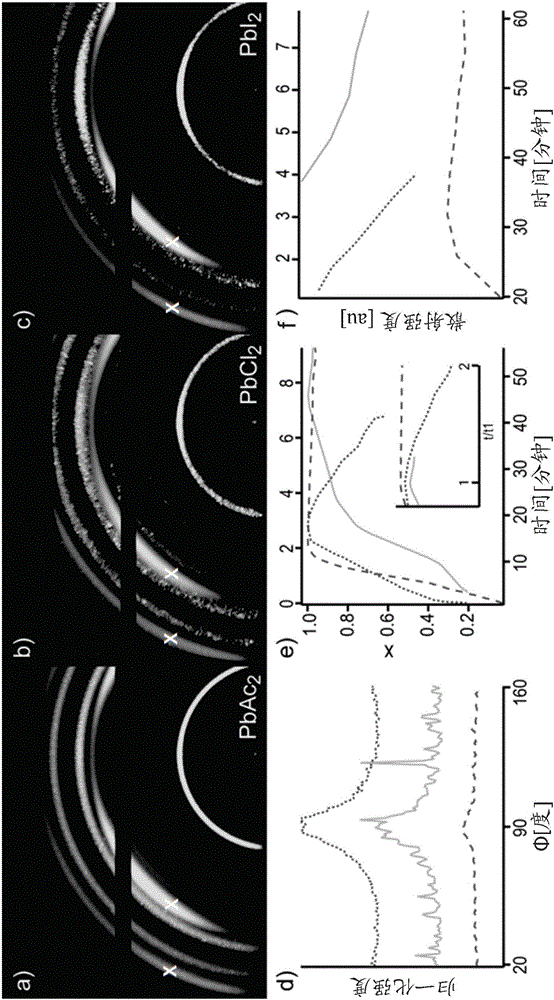
[0375] In addition to having sacrificial anions in the metal salt component to enable crystallization at lower temperatures, some second cations (typically the methylammonium ion of the methylammonium lead halide perovskite) can also be present in the precursor solution Replaced by components that can be "sacrificed" at higher or lower temperatures to affect crystallization. If smaller or lighter cations are chosen, this can enable even faster crystallization to facilitate processing or film uniformity; or slower crystallization to grow larger, higher quality crystals.

[0376] Among the reactions proposed for perovskite crystallization, the example of a mixed halomethylammonium halide lead perovskite: 3MAI+PbCl 2 →MAPbI 3 +2 MACl. It seems that in MAPbI 3 Upon complete crystallization, MA+Cl will be lost in the form of MACl or its decomposition products. Example 1 has shown that the annealing process can be a...


PUM


Abstract

The present invention relates to a process for producing a layer of a crystalline material, which process comprises disposing on a substrate: a first precursor compound comprising a first cation and a sacrificial anion, which first cation is a metal or metalloid cation and which sacrificial anion comprises two or more atoms; and a second precursor compound comprising a second anion and a second cation, which second cation can together with the sacrificial anion form a first volatile compound. The invention also relates to a layer of a crystalline material obtainable by a process according to the invention. The invention also provides a process for producing a semiconductor device comprising a process for producing a layer of a crystalline material according to the invention. The invention also provides a composition comprising: (a) a solvent; (b) NH4X; (c) AX; and (d) BY2 or MY4; wherein X, A, M and Y are as defined herein.

Description

technical field [0001] The invention relates to a method for producing a layer of crystalline material. The layers of crystalline material thus produced can be used in the fabrication of semiconductor devices, such as photovoltaic devices. Also described herein is a method of fabricating a semiconductor device. [0002] The work on the present invention received funding from the European Research Council (FP7 / 2007-2013) / ERC Grant Agreement No. 279881 under the Seventh Framework Program of the European Union. Background technique [0003] Layers and thin films of crystalline materials are important in many applications including the glazing industry, the electronics industry and the photovoltaics industry. It is often important that the above-mentioned layers are smooth and free from holes or defects. Furthermore, it is desirable to be able to manufacture the above-mentioned layers quickly, easily and with minimal expenditure. Layers and films are usually produced by vapo...

Claims


Application Information

Patent Timeline
Patent Type & Authority Applications(China)
IPC IPC(8): H01L51/42H01L51/46H01L51/48
CPCY02E10/549Y02E10/542Y02P70/50H10K71/12H10K71/40H10K85/00H10K30/151H10K85/50C07F7/22C07F7/24C07F1/08H10K30/15H10K71/15H10K71/164H10K71/311H10K30/30H01G9/2009
Inventor 亨利·詹姆斯·施耐德张伟迈克尔·萨利巴
Owner OXFORD UNIV INNOVATION LTD
Why Eureka
Try Eureka