Preparation method for SiGe-based heterogeneous SPiN diode applied to reconfigurable annular antenna

A loop antenna and diode technology, applied in the direction of antenna, radiation element structure, antenna grounding switch structure connection, etc., can solve the problems of large injection dose and energy, impact concentration, incompatibility, etc., to suppress the impact and improve the breakdown voltage Effect

Inactive Publication Date: 2017-06-13
XIAN CREATION KEJI CO LTD
View PDF1 Cites 16 Cited by
  • Summary
  • Abstract
  • Description
  • Claims
  • Application Information

AI Technical Summary

Problems solved by technology

[0003] At present, there is a type of frequency reconfigurable antenna on the market. The material used for the important component SPIN diode is bulk silicon material. This material has the problem of low carrier mobility in the intrinsic region, which affects the current carrying capacity of the intrinsic region of the SPIN diode. subconcentration, thereby affecting its solid-state plasma concentration; and the P region and N region of this structure are mostly formed by implantation process, which requires a large implant dose and energy, requires high equipment, and is not compatible with existing processes; and Diffusion technology is used, although the junction depth is deep, but at the same time, the area of ​​P region and N region is relatively large, the integration degree is low, and the doping concentration is uneven, which affects the electrical performance of SPIN diodes, resulting in poor controllability of solid-state plasma concentration and distribution.

Method used


Image

  • Preparation method for SiGe-based heterogeneous SPiN diode applied to reconfigurable annular antenna
  • Preparation method for SiGe-based heterogeneous SPiN diode applied to reconfigurable annular antenna
  • Preparation method for SiGe-based heterogeneous SPiN diode applied to reconfigurable annular antenna

Examples


Embodiment 1

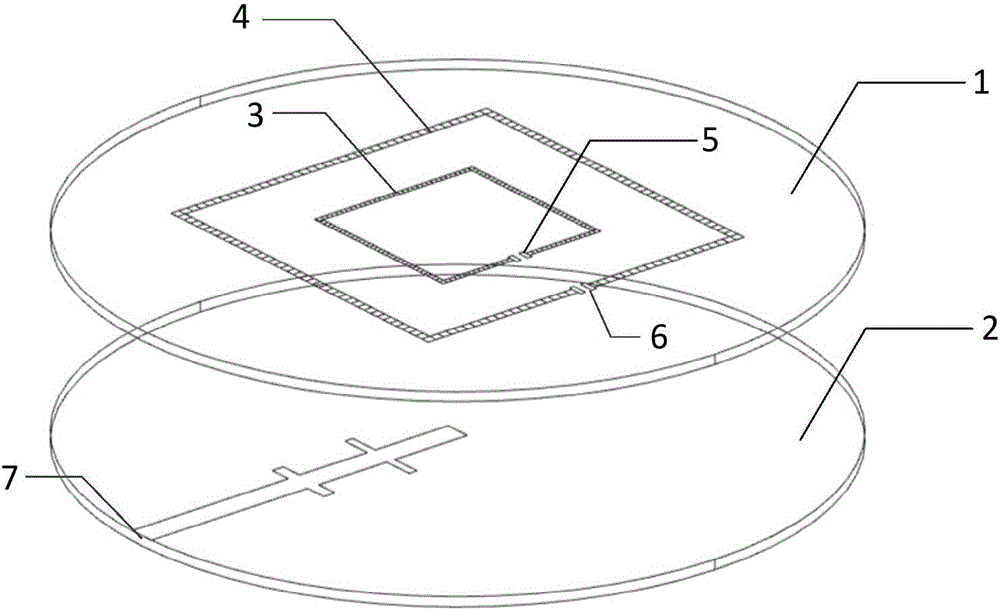
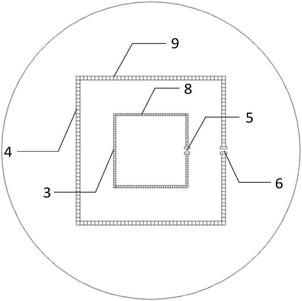
[0060] An embodiment of the present invention provides a method for preparing a SiGe-based heterogeneous SPiN diode for a reconfigurable loop antenna, and the SiGe-based heterogeneous SPiN diode is used to manufacture a reconfigurable loop antenna. Please refer to figure 1 , figure 1 It is a structural schematic diagram of a reconfigurable loop antenna according to an embodiment of the present invention; the loop antenna includes: a semiconductor substrate (1); a dielectric plate (2); a first SPIN diode ring (3), a second SPIN diode ring (4), the first DC bias line (5) and the second DC bias line (6) are all arranged on the semiconductor substrate (1); the coupled feed source (7) is arranged on the On the dielectric plate (2); the first SPIN diode ring (3), the second SPIN diode ring (4), the first DC bias line (5) and the second DC bias line (6) Manufactured on the semiconductor substrate (1) using a semiconductor process.

[0061] Please refer to figure 2 , figure 2 I...

Embodiment 2

[0102] See Figure 7a-Figure 7r , Figure 7a-Figure 7r It is a schematic diagram of a method for preparing a heterogeneous SiGe-based plasma SPIN diode according to an embodiment of the present invention. On the basis of the first embodiment above, to prepare a solid-state plasma SPIN diode with a channel length of 22nm (the length of the solid-state plasma region is 100 microns) As an example to describe in detail, the specific steps are as follows:

[0103] Step 1, substrate material preparation steps:

[0104] (1a) if Figure 7a As shown, the SiGeOI substrate 101 with (100) crystal orientation is selected, the doping type is p-type, and the doping concentration is 1014cm -3 , the thickness of the top layer SiGe is 50 μm;

[0105] (1b) if Figure 7b As shown, the method of chemical vapor deposition (Chemical vapor deposition, referred to as CVD) is used to deposit a layer of first SiO with a thickness of 40 nm on the SiGe layer. 2 layer 201;

[0106] (1c) Deposit a la...

Embodiment 3

[0133] Please refer to Figure 8 , Figure 8 It is a schematic diagram of a device structure of a heterogeneous SiGe-based plasmonic SPIN diode according to an embodiment of the present invention. The heterogeneous SiGe-based plasmonic SPIN diode employs the above-mentioned as figure 2 The preparation method shown is made, specifically, the SiGe-based plasma SPIN diode is prepared and formed on the SiGeOI substrate 301, and the P region 304, the N region 305 of the SPIN diode and the lateral direction are located between the P region 304 and the N region 305 The I-regions between them are located in the top layer SiGe302 of the substrate. Wherein, the SPIN diode can be isolated by STI deep trenches, that is, an isolation trench 303 is provided outside the P region 304 and the N region 305, and the depth of the isolation trench 303 is greater than or equal to the thickness of the top SiGe layer.


PUM


Abstract

The invention relates to a preparation method for a SiGe-based heterogeneous SPiN diode applied to a reconfigurable annular antenna. The preparation method comprises the steps of selecting a SiGeOI substrate of a certain crystal orientation, and setting an isolation region on the SiGeOI substrate; forming a second protection layer on the surface of the SiGeOI substrate; forming a second isolation region pattern on the second protection layer through a photoetching process; etching the second protection layer and the SiGeOI substrate in appointed positions of the second isolation region pattern through a dry etching process to form a P type trench and an N type trench; filling the P type trench and the N type trench, and forming a P type active region and an N type active region in top layer SiGe of the SiGeOI substrate by adopting ion implantation; and forming leads on the SiGeOI substrate to complete the preparation of the SiGe-based heterogeneous SPiN diode. By adoption of the embodiment, the high-performance SiGe-based heterogeneous SPiN diode, which is applicable to formation of the solid-state plasma antenna, can be prepared and provided through a deep trench isolation technology and an ion implantation process.

Description

technical field [0001] The invention relates to the technical field of semiconductor device manufacturing, in particular to a method for preparing a SiGe-based heterogeneous SPiN diode used for a reconfigurable loop antenna. Background technique [0002] In the rapidly developing modern communication system, in order to meet the requirements of communication, navigation, detection, etc., multiple transmitting and receiving antennas need to work on one platform at the same time. In this case, more and more loads and electromagnetic compatibility between antennas become increasingly prominent problems. Reconfigurable antennas can dynamically select different working modes according to different environments, so that one antenna can realize the functions of multiple antennas, and it has made an important exploration for effectively solving the problems of electromagnetic interference and system miniaturization. [0003] At present, there is a type of frequency reconfigurable a...

Claims


Application Information

Patent Timeline
Patent Type & Authority Applications(China)
IPC IPC(8): H01L29/66H01L21/04H01L29/06H01L21/265H01Q1/38H01Q1/50H01Q23/00
Inventor 尹晓雪张亮
Owner XIAN CREATION KEJI CO LTD
Why Eureka
Try Eureka