Gate associated transistor free of polysilicon emitter
A technology of coupled-gate transistors and emitters, which is applied in the manufacture of transistors, semiconductor devices, semiconductor/solid-state devices, etc., can solve problems such as secondary breakdown, high temperature, and high current density, and achieve low dynamic power consumption and high tube temperature. Low, good consistency
- Summary
- Abstract
- Description
- Claims
- Application Information
AI Technical Summary
Problems solved by technology
Method used
Image

Examples
Embodiment Construction
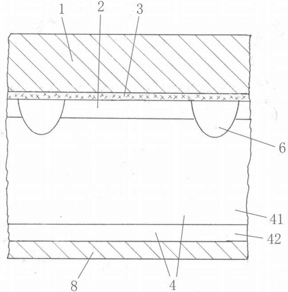
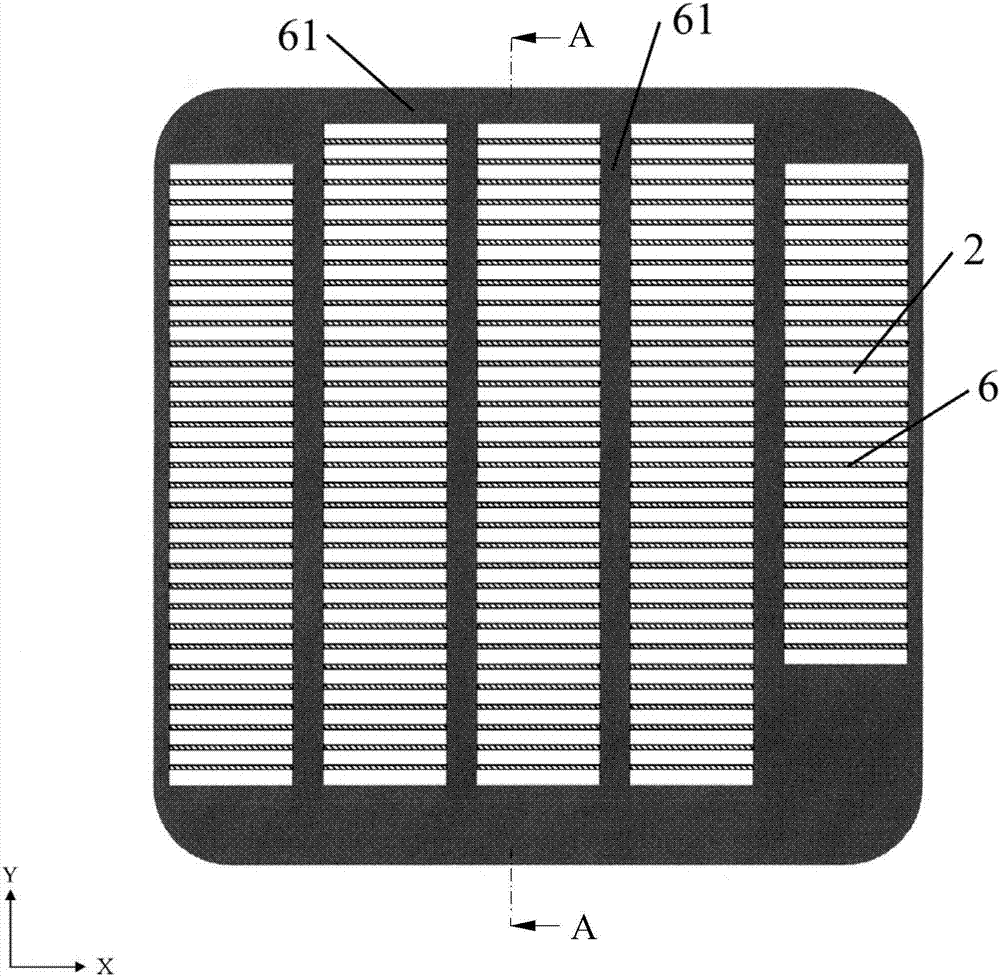
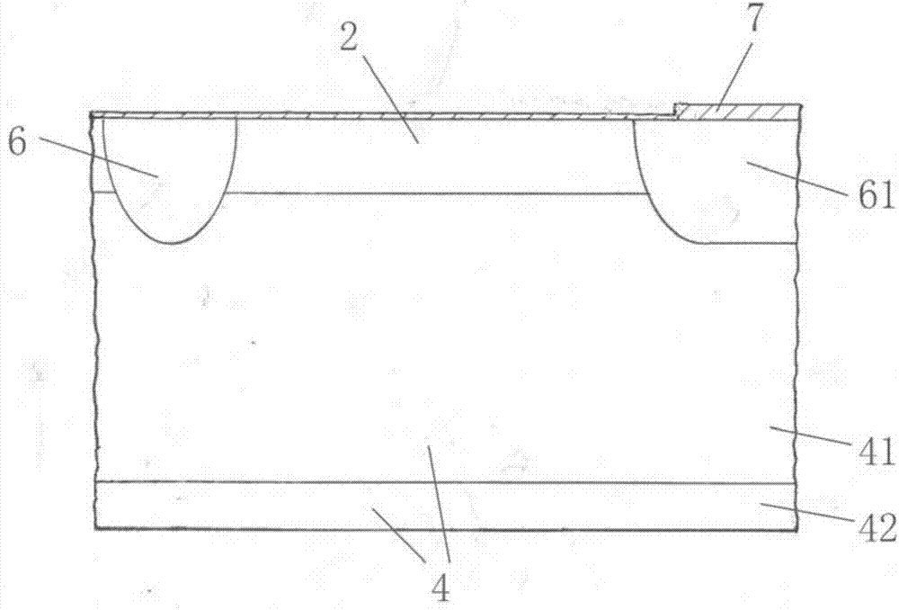
[0042] The invention relates to a connected-gate transistor without a polysilicon emitter and a manufacturing method thereof.
[0043] Figure 1 to Figure 5 It is a structural schematic diagram of an embodiment of a connected-gate transistor without a polysilicon emitter and a process flow diagram along the A-A section of the present invention. The shown structure includes an N-type low-resistivity layer 42 in the lower layer and an N-type high-resistivity layer in the upper layer. The upper surface of the silicon substrate sheet 4 of the rate layer 41 has an N-type emitter region 3 with a high doping concentration. Region 2, the side of the P-type base region 2 is connected to the P-type concentrated base region 6 with a higher doping concentration than the P-type base region 2, the P-type concentrated base region 6 is orthogonal to the bus bar 61 in the P-type concentrated base region, and the silicon lining There is a base metal layer 10 above the bottom sheet 4, and the u...
PUM
 Abstract
Description
Claims
Application Information
 - Generate Ideas
- Intellectual Property
- Life Sciences
- Materials
- Tech Scout
- Unparalleled Data Quality
- Higher Quality Content
- 60% Fewer Hallucinations
Browse by: Latest US Patents, China's latest patents, Technical Efficacy Thesaurus, Application Domain, Technology Topic, Popular Technical Reports.
© 2025 PatSnap. All rights reserved.Legal|Privacy policy|Modern Slavery Act Transparency Statement|Sitemap|About US| Contact US: help@patsnap.com