Method for scale rapid preparation of perovskite semiconductor material

A perovskite and semiconductor technology, applied in the field of large-scale and rapid preparation of perovskite semiconductor materials, can solve the problems of difficult removal of structure-inducing reagents, difficult control of particle size, low purity and yield, etc., and achieve clean and pollution-free reaction routes , easy large-scale preparation, low cost effect

Active Publication Date: 2017-07-11
HEFEI UNIV OF TECH
View PDF4 Cites 13 Cited by
  • Summary
  • Abstract
  • Description
  • Claims
  • Application Information

AI Technical Summary

Problems solved by technology

Currently preparing A 4 wxya 6 The most common method is the reverse phase microemulsion method, but its purity and yield are low, and the structure-inducing reagents used are difficult to comple

Method used


Image

  • Method for scale rapid preparation of perovskite semiconductor material
  • Method for scale rapid preparation of perovskite semiconductor material
  • Method for scale rapid preparation of perovskite semiconductor material

Examples


Embodiment 1

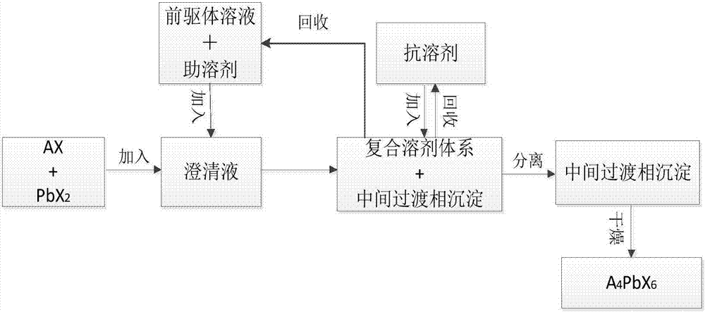
[0023] A large-scale and rapid preparation of perovskite semiconductor material Cs 4 PbBr 6 method, the specific steps are as follows:

[0024] Such as figure 1 shown, using PbBr 2 , CsBr , NH 4 Br as PbX 2 , AX and co-solvent, dimethyl sulfoxide as precursor solution, chloroform as anti-solvent, 1 mol PbBr 2 , 4 mol CsBr dissolved in 20 L containing 2 mol NH 4 Br in the dimethyl sulfoxide solution, stirred until the solution was completely clear to obtain a clear liquid, then quickly added chloroform with the same volume as the clear liquid, and stirred at the same time, a white intermediate transition phase precipitate was generated in the system, and then centrifuged, the solvent Recycled into the next cycle of production, the obtained intermediate transition phase precipitate was dried at a constant temperature of 60 °C for 1 hour to obtain yellow-green Cs 4 PbBr 6 powder, the yield reaches 100%, and the quantum yield reaches 90%.

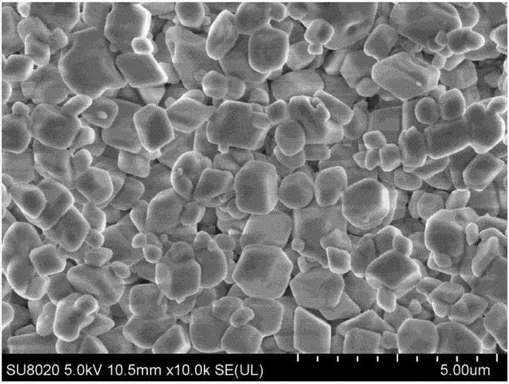
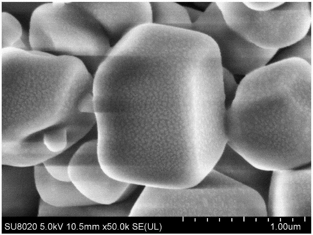
[0025] figure 2 It is the SE...

Embodiment 2

[0027] A large-scale and rapid preparation of perovskite semiconductor material Cs 4 PbBr 6 method, the specific steps are as follows:

[0028] Such as figure 1 shown, using PbBr 2 , CsBr, HBr as PbX 2 , AX and co-solvent, dimethyl sulfoxide as precursor solution, chloroform as anti-solvent, 1 mol PbBr 2 , 0.5 mol CsBr was dissolved in 5 L of dimethyl sulfoxide solution containing 2 mol HBr, stirred until the solution was completely clear to obtain a clear liquid, then quickly added chloroform with the same volume as the clear liquid, while stirring, the system formed The white precipitate was then centrifuged, and the solvent was recovered for use in the next cycle of production. The obtained white precipitate was kept at 60 °C for 1 hour to obtain yellow-green Cs 4 PbBr 6 powder and white PbBr 2 Powder mixture, PbBr removed with DMSO 2 powder to give yellow-green Cs 4 PbBr 6 , the yield was 40%, and the quantum yield reached 30%.

Embodiment 3

[0030] A large-scale and rapid preparation of perovskite Cs 4 PbBr 6 method, the specific steps are as follows:

[0031] Such as figure 1 shown, using PbBr 2 , CsBr as PbX 2 , AX, HBr as co-solvent, DMSO as precursor solution, chloroform as anti-solvent, 1 mol PbBr 2 10 mol CsBr was dissolved in 25 L of dimethyl sulfoxide solution containing 2 mol HBr, stirred until the solution was completely clear to obtain a clear liquid, then quickly added chloroform with the same volume as the clear liquid, while stirring, the system formed The white precipitate was then centrifuged, and the solvent was recovered for use in the next cycle of production. The obtained white precipitate was kept at 60 °C for 1 hour to obtain yellow-green Cs 4 PbBr 6 Mixed powder with white CsBr, Cs 4 PbBr 6 The yield rate was 20%, and the quantum yield reached 40%.


PUM


Abstract

The invention discloses a method for scale rapid preparation of a perovskite semiconductor material, wherein the method comprises the specific steps: dissolving or partially dissolving PbX2 and AX in a precursor solvent according to a certain proportion to obtain a precursor solution system; then adding a cosolvent, to obtain a clarified liquid; followed by, adding an anti solvent, and carrying out fast stirring reaction to generate an intermediate transition phase precipitate; and then carrying out drying treatment of the intermediate transition phase precipitate for 1 min-10 h at room temperature-100 DEG C, to obtain high-purity A4PbX6, wherein A is Cs<+>, Ru<+>, a methylamine cation, a formamidine cation or a mixed cation thereof, and X is a halogen ion. All the anti solvent, the precursor solvent and the co-solvent and the like used in the preparation process can be recovered and continue to use in next circulating production; circulation and no emissions are achieved in the whole preparation process, high yield and scale preparation of the product are achieved, the product has high fluorescence quantum yield, and the cost is low.

Description

technical field [0001] The invention relates to the technical field of perovskite material preparation, in particular to a method for rapidly preparing perovskite semiconductor materials on a large scale. Background technique [0002] With people's increasing concern on clean energy, functional optoelectronic materials have become an increasing demand in basic science and application fields. Perovskite A 4 wxya 6 It is a kind of functional semiconductor material. Due to its excellent optoelectronic and optical characteristics, such as high quantum efficiency, chromatographic purity, narrow emission line width and wide wavelength tunability, etc., it is considered to be widely used in the fields of lasers, photodiodes, photodetectors, photovoltaics and photoluminescence. It has great application potential. Currently preparing A 4 wxya 6 The most common method is the reverse phase microemulsion method, but its purity and yield are low, and the structure-inducing reagents...

Claims


Application Information

Patent Timeline
IPC IPC(8): C01G21/16C09K11/66
CPCC01G21/006C01G21/16C01P2002/72C01P2002/80C01P2004/03C09K11/665
Inventor 刘节华魏香凤
Owner HEFEI UNIV OF TECH
Why Eureka
Try Eureka