Graphene field-effect transistor and formation method thereof

A field effect transistor and graphene technology, which is applied in semiconductor devices, semiconductor/solid-state device manufacturing, electrical components, etc., can solve the problems of affecting the electrical performance of the device, and achieve easy control of the preparation process, simplification of the preparation process, and high current carrying capacity. The effect of sub-mobility

Active Publication Date: 2017-07-14
SEMICON MFG INT (SHANGHAI) CORP +1
View PDF3 Cites 7 Cited by
  • Summary
  • Abstract
  • Description
  • Claims
  • Application Information

AI Technical Summary

Problems solved by technology

However, both methods have obvious disadvantages, because some non-ideal factors, such as wrinkles, holes, impurities, etc., will inevitably be introduced during the graphene transf...

Method used


Image

  • Graphene field-effect transistor and formation method thereof
  • Graphene field-effect transistor and formation method thereof
  • Graphene field-effect transistor and formation method thereof

Examples


Embodiment Construction

[0028] The present invention provides a graphene field effect transistor and its forming method, which will be described in detail below in conjunction with the accompanying drawings.

[0029] Figure 1 to Figure 9 It is a cross-sectional schematic diagram of an intermediate structure of a method for forming a graphene field effect transistor according to an embodiment of the present invention.

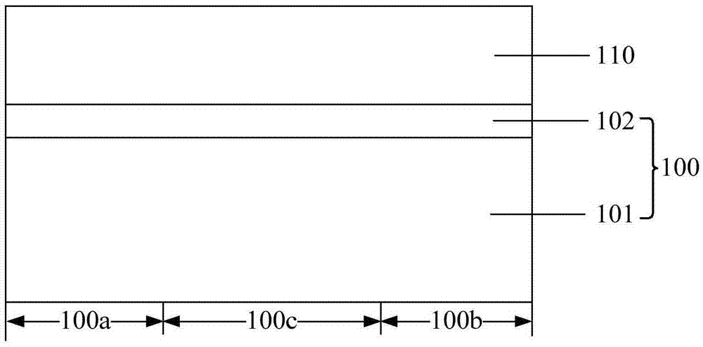
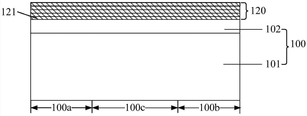
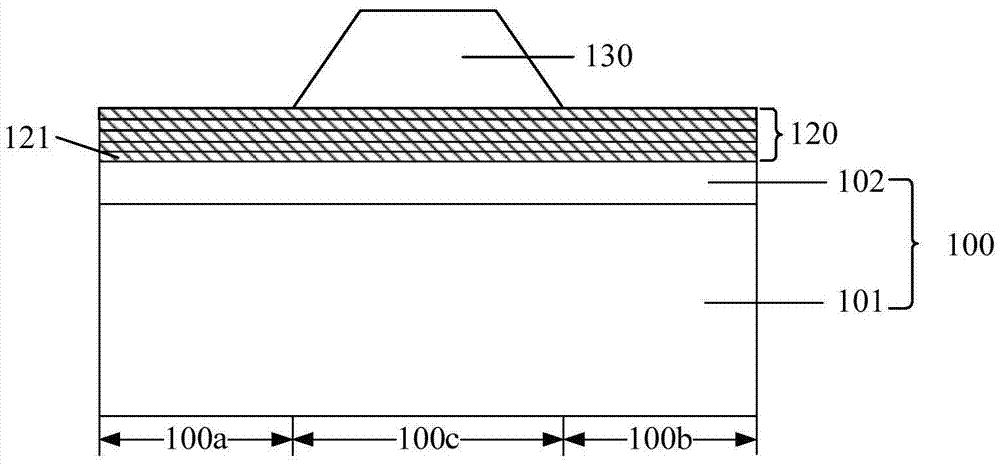
[0030] refer to figure 1 , providing a substrate 100, the substrate 100 includes a first region 100a, a second region 100b, and a third region 100c between the first region 100a and the second region 100b; the substrate 100 includes a substrate 101 and a liner 102 , the lining layer 102 is formed on the substrate 101 ; and the graphite material layer 110 is formed on the substrate 100 .

[0031] In the embodiment of the present invention, the substrate 101 may be a silicon substrate, a silicon germanium substrate, a silicon carbide substrate, a silicon-on-insulator substrate, a germ...


PUM

PropertyMeasurementUnit
Thicknessaaaaaaaaaa

Abstract

The invention relates to a graphene field-effect transistor and a formation method thereof. The formation method of the graphene field-effect transistor comprises the steps of providing a substrate, wherein the substrate comprises a first region, a second region and a third region, and the third region is arranged between the first region and the second region; forming a graphite material layer on the substrate; processing the graphite material layer to form multi-layer graphene; removing a part of multi-layer graphene on the first region and the second region from a thickness direction to form single-layer graphene or dual-layer graphene; forming a gate dielectric layer on a surface of the multi-layer graphene on the third region; removing a part of the single-layer graphene or the dual-layer graphene on the first region and the second region to respectively form a source region and a drain region; and respectively forming electrodes on the source region, the drain region and the gate dielectric layer. With the formation method disclosed by the embodiment of the invention, the in-situ growth of the graphene is achieved, a graphene preparation method from top to bottom is employed, the process is simplified, and the process is easy to control.

Description

technical field [0001] The invention relates to the technical field of semiconductor manufacturing, in particular to a graphene field effect transistor and a forming method thereof. Background technique [0002] Graphene is a new type of two-dimensional nanomaterial with a planar benzene ring structure. The thickness of a single layer of graphene is only about one atomic layer thick; due to its zero-gap energy band structure, the electron mobility at room temperature can reach three times the speed of light. One percent, lower resistivity than copper or silver, and thanks to the chemical bonds between carbon atoms, graphene is a hundred times stronger mechanically than steel. It is precisely because of these excellent properties exhibited by the special structure of graphene that graphene has been used in transistors, transparent electrodes, display screens, supercapacitors, solar cells and other fields, and achieved good results. [0003] However, since single-layer graphe...

Claims


Application Information

Patent Timeline
IPC IPC(8): H01L29/16H01L21/336H01L29/78
CPCH01L29/1606H01L29/66015H01L29/78
Inventor 郑喆张海洋
Owner SEMICON MFG INT (SHANGHAI) CORP
Why Eureka
Try Eureka