Fully-differential amplifier and residual gain circuit using fully-differential amplifier

A fully differential amplifier and gain circuit technology, applied in the direction of differential amplifiers, amplifiers, amplification control, etc., can solve the problems of low power consumption, gain reduction, gain high speed, etc., achieve fast charge and discharge characteristics, and improve DC gain , the effect of increasing the equivalent gain

Active Publication Date: 2017-07-14
INST OF MICROELECTRONICS CHINESE ACAD OF SCI
View PDF4 Cites 5 Cited by
  • Summary
  • Abstract
  • Description
  • Claims
  • Application Information

AI Technical Summary

Problems solved by technology

As shown in Figure 1(a), it is a telescopic cascode OTA, which has a large gain, the fastest speed, and the lowest power consumption, but its input and output swings are the smallest. When connected to unity gain, it works The range is very small; Figure 1(b) is a folded cascode OTA, which has a large input and output swing, but its power consumption is double that of the telescopic cascode OTA, and the noise The performance and gain are also worse than the sleeve-type cascode OTA; Figure 1(c) is a two-stage (Two-Stage) OTA, its gain and output swing are large, but its frequency response is the worst, usually need to block capacitor (RC) compensation network, and the power consumption is the largest among the three types of OTA
With the continuous development of CMOS technology, especially when the power supply voltage is reduced below 1V, the intrinsic gain of the transistor drops rapidly, and the input and output swings of the sleeve OTA and the folding OTA are severely limited, and their gain is also greatly reduced. Its performance can no longer meet the requirements of low-voltage design; two-level OTA can meet the above requirements, but its power consumption is the largest, which does not meet the design concept of low power consumption
Usually, the way to solve the gain problem is to introduce gain-boosting technology on the cascode tube in the telescopic OTA and folded OTA to improve the open-loop gain of the OTA, but this technology will introduce complex frequency response, the increased power consumption is also larger

Method used


Image

  • Fully-differential amplifier and residual gain circuit using fully-differential amplifier
  • Fully-differential amplifier and residual gain circuit using fully-differential amplifier
  • Fully-differential amplifier and residual gain circuit using fully-differential amplifier

Examples


Embodiment 1

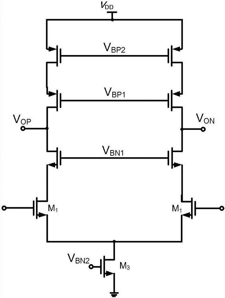
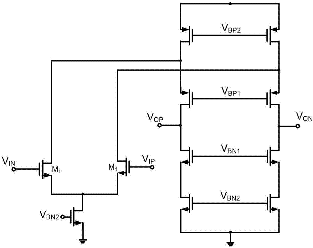
[0052] Such as Figure 4 As shown, this embodiment proposes a fully differential amplifier, including a first complementary differential input pair 101, a second complementary differential input pair 102, and all connected to the first complementary differential input pair 101 and the second complementary differential input pair 102 The first tail current source 104 and the second tail current source 105, the fully differential amplifier also includes a positive feedback system 103, connected with the first complementary differential input pair 101 and the second complementary differential input pair 102, for providing the first complementary differential input pair The input pair 101 and the second complementary differential input pair 102 provide positive feedback.

[0053] Specifically, the first complementary differential input pair 101 has two equal-sized and complementary MOS transistors M1A and M1B, and the gates of the two MOS transistors M1A and M1B are connected to t...

Embodiment 2

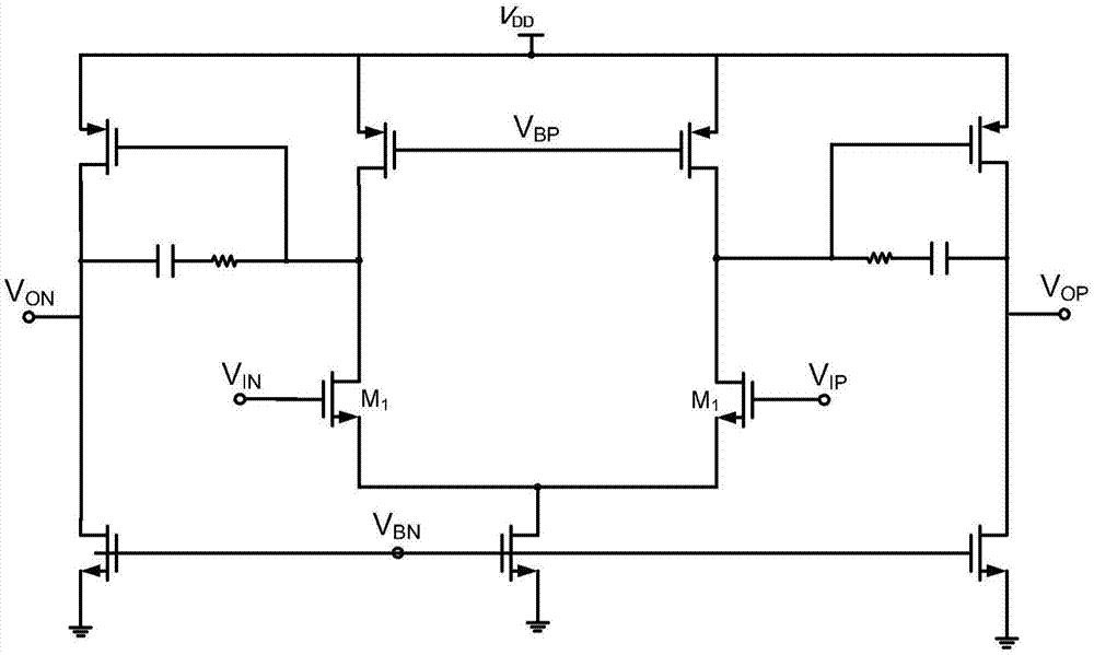
[0062] Such as Figure 6 As shown, this embodiment proposes a residual gain circuit (MDAC), which uses the fully differential amplifier in Embodiment 1 (see Figure 6 The structure inside the dotted line frame), and introduces the CLS technology to improve the equivalent gain of the amplifier. C1 and C2 are sampling capacitors of the same size, and the output of MDAC can achieve 2V IN -V DAC , where V IN is the input voltage, V DAC is the output voltage of the sub-digital-to-analog converter (Sub-DAC).

[0063] Since when the output of the amplifier reaches the maximum swing, the third complementary differential input pair M3A and M3B of the positive feedback system may enter the linear region, which will cause the gain of the amplifier to drop. However, with the help of the CLS method, the final output of the amplifier can always be stable at the common-mode output level V CM Nearby, the gain of the amplifier is maintained, thereby reducing the gain nonlinearity.

[00...


PUM


Abstract

The invention relates to a fully-differential amplifier. The fully-differential amplifier comprises first and second complementary differential input pairs, and further comprises a positive feedback system; the positive feedback system is connected with the first and second complementary differential input pairs, and used for providing positive feedback to the first complementary differential input pair and the second complementary differential input pair; the positive feedback system comprises a third complementary differential input pair; the third complementary differential input pair comprises a first PMOS transistor and a second PMOS transistor; the grids of the first PMOS transistor and the second PMOS transistor are separately connected with the output ends of the first complementary differential input pair and the second complementary differential input pair; and the drains of the first PMOS transistor and the second PMOS transistor are separately connected with the output ends of the second complementary differential input pair and the first complementary differential input pair. On the basis of the fully-differential amplifier, the invention further provides a residual gain circuit adopting a related level shift method. The fully-differential amplifier disclosed by the invention has the advantages of being low in power consumption, rapid in speed, high in conversion rate and simple in circuit structure; and, with the help of the related level shift technology, the high-speed and high-precision residual gain circuit can be realized.

Description

technical field [0001] The invention belongs to the field of analog-to-digital converters, and more specifically relates to a fully differential amplifier and a residual gain circuit using the same. Background technique [0002] Pipeline analog-to-digital converter (ADC) is a kind of high-speed and high-precision analog-to-digital converter, which is widely used in communication systems and complementary metal oxide semiconductor (CMOS) image sensors. In the traditional pipeline ADC design, the transconductance operational amplifier (OTA) accounts for the main part of the power consumption in the analog domain. Therefore, designing a high-performance OTA is crucial to the entire ADC. [0003] Existing OTAs are generally divided into telescopic OTAs, foldable OTAs, and two-stage OTAs. As shown in Figure 1(a), it is a telescopic cascode OTA, which has a large gain, the fastest speed, and the lowest power consumption, but its input and output swings are the smallest. When conn...

Claims


Application Information

Patent Timeline
Patent Type & Authority Applications(China)
IPC IPC(8): H03F1/38H03F3/45H03G3/30H03M1/12
CPCH03F1/38H03F3/45179H03G3/3036H03G3/3084H03M1/1245
Inventor 陈鸣陈敏陈杰
Owner INST OF MICROELECTRONICS CHINESE ACAD OF SCI
Why Eureka
Try Eureka