Film solar cell with combination of perovskite monocrystalline material and P-type monocrystalline silicon and preparation method thereof

A technology of thin-film solar cells and single-crystal materials, applied in circuits, photovoltaic power generation, electrical components, etc., can solve the problems of low photoelectric conversion performance, insufficient stability, and easy to be affected, so as to avoid high production costs and avoid production. The process is cumbersome and the effect of improving instability

Pending Publication Date: 2017-07-21
HEBEI UNIV OF TECH
View PDF8 Cites 2 Cited by
  • Summary
  • Abstract
  • Description
  • Claims
  • Application Information

AI Technical Summary

Problems solved by technology

There are many grains, grain boundaries, pores and surface defects in the mixed phase film of amorphous and microcrystalline, which will cause the recombination of carriers, and the perovskite in the film state has high sensitivity to temperature, humidity and gas. Responsive, easily affected, loses its original properties
Therefore, the current solar cells combined with perovskite and silicon have the disadvantages of low photoelectric conversion performance and insufficient stability.

Method used


Image

  • Film solar cell with combination of perovskite monocrystalline material and P-type monocrystalline silicon and preparation method thereof
  • Film solar cell with combination of perovskite monocrystalline material and P-type monocrystalline silicon and preparation method thereof

Examples


Embodiment 1

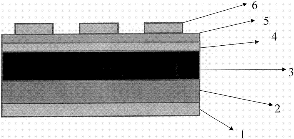
[0057] A thin-film solar cell combined with perovskite single crystal material and P-type single crystal silicon, consisting of a bottom electrode, a dense zinc dioxide layer, C 60 Electronic thin film layer, single crystal perovskite light absorption layer, single crystal silicon hole transport layer, top electrode these six parts are matched with each other and combined together, constitute the combination of perovskite single crystal material and P-type single crystal silicon of the present invention thin film solar cells. The C 60 The electron thin film layer was evaporated on the surface of the perovskite single crystal, and the dense ZnO electron transport layer was sputter deposited on the C 60 On the surface of the electronic thin film layer, the single crystal silicon hole transport layer is deposited on the surface of the perovskite single crystal, and the film composed of aluminum or silver is plated on the surface of the dense ZnO electron transport layer and the ...

Embodiment 2

[0075] A thin-film solar cell combined with perovskite single crystal material and P-type single crystal silicon, consisting of a bottom electrode, a dense zinc dioxide layer, C 60 Thin film layer, single-crystal perovskite light-absorbing layer, single-crystal silicon hole-transporting layer, and top electrodes are combined together to form the combination of perovskite single-crystal material and P-type single-crystal silicon of the present invention. thin film solar cells. The C 60 The electronic thin film layer is evaporated on the surface of the perovskite single crystal, the dense ZnO electron transport layer is sputter deposited on the surface of the C60 electronic thin film layer, and the single crystal silicon hole transport layer is deposited to cover the perovskite single crystal. On the surface, films composed of aluminum or silver are plated on the surface of the dense ZnO electron transport layer and hole transport layer to form the bottom and top electrodes.

...

Embodiment 3

[0093] A thin-film solar cell combined with perovskite single crystal material and P-type single crystal silicon, consisting of a bottom electrode, a dense zinc dioxide layer, a C60 thin film layer, a single crystal perovskite light absorption layer, a single crystal silicon hole transport layer, and a top The six parts of the electrode and the electrode are matched and compounded together to form a thin-film solar cell in which the perovskite single crystal material and P-type single crystal silicon are combined in the present invention. The C60 electronic thin film layer is vapor-deposited on the surface of the perovskite single crystal, the dense ZnO electron transport layer is deposited on the surface of the C60 electronic thin film layer by sputtering, and the single crystal silicon hole transport layer is deposited to cover the perovskite On the surface of the ore single crystal, a film composed of aluminum or silver is plated on the surface of the dense ZnO electron tran...


PUM

PropertyMeasurementUnit
Thicknessaaaaaaaaaa
Thicknessaaaaaaaaaa
Thicknessaaaaaaaaaa

Abstract

The present invention provides a film solar cell with the combination of a perovskite monocrystalline material and P-type monocrystalline silicon, and relates to a semiconductor device for converting luminous energy to electric energy. The film solar cell with the combination of the perovskite monocrystalline material and the P-type monocrystalline silicon is formed by a bottom electrode, an N-type oxide semiconductor film, a C<60> electronic film, a perovskite monocrystalline luminous absorption layer, a monocrystalline silicon hole transport layer, and top electrodes, the oxide semiconductor film is an N-type zinc oxide film obtained through magnetron sputtering, the C<60> electronic film is a buffer layer obtained through thermal evaporation, the perovskite monocrystalline is a luminous absorption material with a perovskite structure, the hole transport layer is a P-type monocrystalline silicon material obtained through magnetron sputtering, and the bottom electrode and the top electrodes are films formed by aluminum or silver and obtained through thermal evaporation. According to the film solar cell, the perovskite monocrystalline material is regarded as the luminous absorption layer, the P-type monocrystalline silicon material is regarded as the hole transport layer, and the stable and high-efficiency solar cell is obtained.

Description

technical field [0001] The technical solution of the invention relates to a semiconductor device specially suitable for converting light energy into electric energy, specifically a thin-film solar cell combined with perovskite single crystal material and P-type single crystal silicon and its preparation method. Background technique [0002] The use of solar energy is a major breakthrough in the progress of human society. With the decline of fossil fuels, solar energy has become an important part of energy used by human beings and has been continuously developed. As a renewable energy source, solar energy is mainly used to convert solar energy into electrical energy, which is then applied to all aspects of human life. Low-cost, high-efficiency and long-term stable solar cells are the basis for realizing large-scale photoelectric conversion using solar energy. [0003] One type of solar cell is a monocrystalline silicon solar cell. This battery has good stability and is curr...

Claims


Application Information

Patent Timeline
IPC IPC(8): H01L51/42H01L51/46
CPCH10K85/30H10K30/451H10K2102/00Y02E10/549
Inventor 田汉民金慧娇田学民戎小莹张天郭丹赵昆越
Owner HEBEI UNIV OF TECH
Why Eureka
Try Eureka