Three-dimensional ceramic substrate comprising cavity structure and fabrication method of three-dimensional ceramic substrate

A technology of ceramic substrate and cavity, which is applied in the field of three-dimensional ceramic substrate with cavity structure and its preparation, can solve the problems of difficult packaging materials and process compatibility, limited mass production and application, high cost, etc., and achieves good fluidity, material Low cost and good heat resistance

Active Publication Date: 2017-07-25
武汉利之达科技股份有限公司
View PDF5 Cites 7 Cited by
  • Summary
  • Abstract
  • Description
  • Claims
  • Application Information

AI Technical Summary

Problems solved by technology

However, the existing substrate cavity structures are generally prepared by high-temperature processes (such as LTCC and HTCC), which are difficult to be compatible with existing packaging materials and processes, and the cost is high, which limits its mass production and application

Method used


Image

  • Three-dimensional ceramic substrate comprising cavity structure and fabrication method of three-dimensional ceramic substrate
  • Three-dimensional ceramic substrate comprising cavity structure and fabrication method of three-dimensional ceramic substrate
  • Three-dimensional ceramic substrate comprising cavity structure and fabrication method of three-dimensional ceramic substrate

Examples


preparation example Construction

[0046] A method for preparing a three-dimensional ceramic substrate with a cavity structure according to an embodiment of the present invention specifically includes:

[0047] (1) preparing a planar ceramic substrate containing metal circuits;

[0048] (2) Design and prepare a mold according to the cavity structure and size requirements, and the mold material is plastic, rubber or other polymer materials;

[0049] (3) cleaning the planar ceramic substrate and the mould, and aligning the planar ceramic substrate with the mould;

[0050] (4) Prepare low-temperature curing ceramic slurry. Low-temperature curing ceramic slurry is a kind of inorganic material slurry, which is composed of water, oxide and phosphate materials in proportion. High strength (compressive strength greater than 30MPa), good heat resistance, corrosion resistance and other advantages. In particular, the ceramic slurry can be cured at room temperature or below 100 degrees to meet the requirements of direct...

Embodiment 1

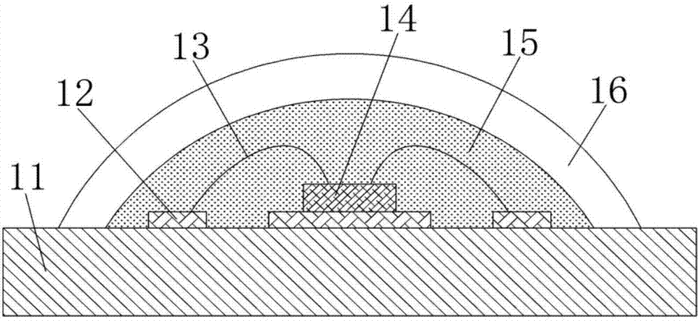
[0055] Fig. 6(a) is a schematic structural diagram of a three-dimensional ceramic substrate with a cavity structure according to an embodiment of the present invention, Figure 10 It is a schematic diagram of a three-dimensional ceramic substrate with a cavity structure according to an embodiment of the present invention, as shown in Figure 6(a) and Figure 10 As shown, Embodiment 1 provides a three-dimensional ceramic substrate with a cavity structure, including an electroplated ceramic substrate 60 and a cavity structure 61 . Wherein, the electroplated ceramic substrate includes a ceramic substrate 62, a metal circuit 63 and a metal through hole 64; the cavity is located on the ceramic substrate 62 and the metal circuit 63, and is an annular structure, and the inner diameter of the annular cavity is 2mm. The outer diameter is 3mm and the height is 0.3mm.

[0056] A method for preparing a three-dimensional ceramic substrate with a cavity structure in Example 1, comprising: ...

Embodiment 2

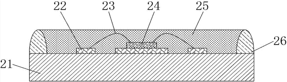
[0065] As shown in FIG. 12( a ), Embodiment 2 provides a three-dimensional ceramic substrate with a cavity structure, including a planar ceramic substrate and a cavity structure 123 . Wherein, the planar ceramic substrate is a thick film ceramic substrate (TFC), including a ceramic substrate 121 and a metal circuit 122; the cavity is located on the ceramic substrate 121 and the metal circuit 122, and is a square ring structure with a side length of 5mm. The ring width is 1mm and the height is 1.0mm.

[0066] A method for preparing a three-dimensional ceramic substrate with a cavity structure according to embodiment 2, comprising:

[0067] (1) Prepare a thick film ceramic substrate (TFC) with metal circuits on the surface;

[0068] (2) According to the cavity structure requirements, process the metal mold (die), and then obtain the polytetrafluoroethylene mold by the mold transfer method;

[0069] (3) Use ethanol and deionized water to clean the thick-film ceramic substrate a...


PUM

PropertyMeasurementUnit
compressive strengthaaaaaaaaaa
heightaaaaaaaaaa
lengthaaaaaaaaaa

Abstract

The invention discloses a three-dimensional ceramic substrate comprising a cavity structure. The three-dimensional ceramic substrate comprises a planar ceramic substrate and the cavity structure attached onto the planar ceramic substrate. The invention also discloses a fabrication method of the three-dimensional ceramic substrate. The fabrication method comprises the steps of firstly, fabricating the planar ceramic substrate with a surface comprising a metal circuit, designing and fabricating a die according to the cavity structure and the size requirement, and fabricating low-temperature cured ceramic paste; secondly, combining the die after the planar ceramic substrate and a plastic die are aligned, and uniformly filling the ceramic paste in a die cavity by modes such as mechanical vibration, pressure injection or vacuum pumping; and finally, allowing to stand for 15-60 minutes under a room temperature or a low temperature (lower than 100 DEG C), and removing the die after the paste is cured. The three-dimensional ceramic substrate has good thermal resistance, corrosion resistance and sealing performance; and the fabrication method of the three-dimensional ceramic substrate has the advantages of low material cost, simple process and high pattern accuracy, particularly, the ceramic paste can be cured under the room temperature or the temperature lower than 100 DEG C, and the hermetical package demands of white-light LED, ultraviolet-light LED and other electrical devices are satisfied.

Description

technical field [0001] The invention belongs to the field of electronic manufacturing, and in particular relates to a three-dimensional ceramic substrate with a cavity structure and a preparation method thereof. Background technique [0002] Compared with traditional lighting sources (incandescent lamps, fluorescent lamps, etc.), white LEDs (Light Emitting Diodes) have the advantages of high light efficiency, long service life, energy saving and environmental protection. At present, white light LEDs generally use blue LED chips to excite yellow phosphors to obtain white light. like figure 1 As shown, a white LED module generally includes a blue LED chip, an adhesive layer containing phosphor powder, gold wires, lenses, a heat dissipation substrate, and a metal circuit layer. The main purpose of adding a lens is to improve the light output efficiency and reliability of the module, which is usually prepared by an expensive mold top (Molding) process. Since the phosphor powd...

Claims


Application Information

Patent Timeline
Patent Type & Authority Applications(China)
IPC IPC(8): H01L23/15H01L23/13H01L21/48H01L33/48H01L33/62
CPCH01L21/4807H01L23/13H01L23/15H01L33/486H01L33/62H01L2224/48091H01L2224/48227H01L2924/181H01L2924/00014H01L2924/00012
Inventor 陈明祥程浩郝自亮刘松坡
Owner 武汉利之达科技股份有限公司
Why Eureka
Try Eureka