Polishing method of ultrathin wafer
A wafer, ultra-thin technology, applied in the manufacturing of electrical components, electric solid-state devices, semiconductor/solid-state devices, etc., can solve the problems of increased capital investment, small output of wax-based processes, and inability to meet market demands, and achieves the The effect of high mechanical strength
- Summary
- Abstract
- Description
- Claims
- Application Information
AI Technical Summary
Problems solved by technology
Method used
Image

Examples
Embodiment 1
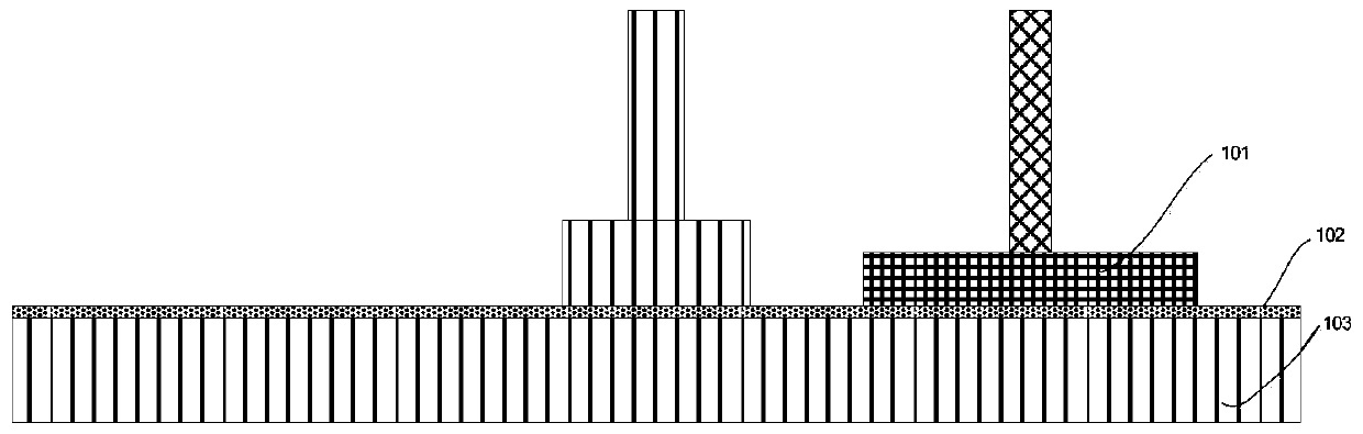
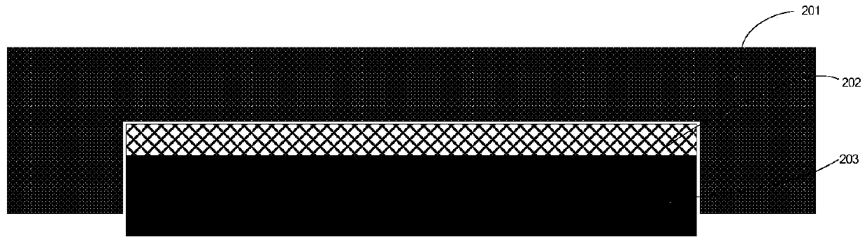
[0042] (1) if image 3 As shown, for an ultra-thin wafer, its thickness is not enough to meet the thickness requirements of embedding the template 201 or exposing the thickness of the template 201 during grinding. Here, a layer of adhesive tape is first attached to the non-polished surface of the wafer 203 to form a film-attached wafer with an increased overall thickness. , the adhesive tape is composed of two parts, that is, an adhesive film 302 and a surface film 301 that provides mechanical force. The surface film 301 is combined with the wafer 203 through an adhesive film 302, where the adhesive film 302 can be a resinous (such as polyurethane) viscous substance, and the adhesive film 302 is heated, photon radiation, laser radiation, electron radiation, and sound wave radiation. or other radiation methods, its viscosity will decrease or disappear; here the surface film 301 can be polyacrylic, polyethylene plastic film, or metal film (aluminum, tin, copper) and so on. The ...
Embodiment 2
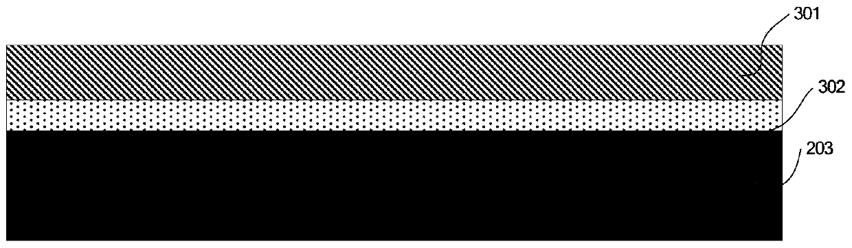
[0047] (1) if Figure 6 Shown, first at wafer 203 non-polishing surface coating colloid 401, this colloid 401 can be coated with spin coating method, also can be coated with film method, also can be coated with glue spraying method; Colloid 401 after coating It can be cured directly, or it can be cured by leveling the surface after baking; the curing method can be heating, photon radiation, laser radiation, electron radiation, sound wave radiation or other radiation methods; the thickness of the colloid 401 is 10nm~1500μm; the colloid The material of 401 can be polyacrylate organic matter, phenolic resin organic matter, epoxy resin organic matter, etc.
[0048] The colloid 401 can lose colloidal properties through heating, photon radiation, laser radiation, electron radiation, sonic radiation or other radiation methods, and can be removed by water washing, plasma oxidation, or immersion in organic degumming solution; the colloid 401 can also be cured A film is formed, which c...
Embodiment 3
[0053] (1) if Figure 9 Shown, first at wafer 203 non-polishing surface coating colloid 401, this colloid 401 can be coated with spin coating method, also can be coated with film method, also can be coated with glue spraying method; Colloid 401 after coating It can be cured directly, or it can be cured after leveling the surface after baking; the curing method can be heating, photon radiation, laser radiation, electron radiation, sound wave radiation or other radiation methods. The thickness of colloid 401 is 10nm~1500μm. The material of the colloid 401 can be polyacrylate organic matter, phenolic resin organic matter, epoxy resin organic matter, and the like.
[0054] The colloid 401 can lose colloidal properties through heating, photon radiation, laser radiation, electron radiation, sonic radiation or other radiation methods, and can be removed by water washing, plasma oxidation, or immersion in organic degumming solution; the colloid 401 can also be cured A film can be fo...
PUM
 Abstract
Description
Claims
Application Information
 - R&D
- Intellectual Property
- Life Sciences
- Materials
- Tech Scout
- Unparalleled Data Quality
- Higher Quality Content
- 60% Fewer Hallucinations
Browse by: Latest US Patents, China's latest patents, Technical Efficacy Thesaurus, Application Domain, Technology Topic, Popular Technical Reports.
© 2025 PatSnap. All rights reserved.Legal|Privacy policy|Modern Slavery Act Transparency Statement|Sitemap|About US| Contact US: help@patsnap.com