GaN nanometer column grown on Si(111) substrate and preparation method and application thereof

A nano-column and substrate technology, applied in the field of GaN nano-columns, can solve the problems of uneven distribution of GaN nano-columns, large lattice mismatch and thermal mismatch, and uneven diameter length, so as to improve the disorder of column direction, The effect of low defect density and short production cycle

Active Publication Date: 2017-08-15
SOUTH CHINA UNIV OF TECH
View PDF3 Cites 6 Cited by
  • Summary
  • Abstract
  • Description
  • Claims
  • Application Information

AI Technical Summary

Problems solved by technology

However, due to the large lattice mismatch and thermal mismatch between Si and GaN; at the same time, the distribution of GaN nanocolumns is not uniform in the early stage of growth, and the difference in the distribution of Ga and N atoms during the growth process leads to the growth of GaN nanocolumns. , uneven diameter length, poor order, etc.

Method used


Image

  • GaN nanometer column grown on Si(111) substrate and preparation method and application thereof
  • GaN nanometer column grown on Si(111) substrate and preparation method and application thereof
  • GaN nanometer column grown on Si(111) substrate and preparation method and application thereof

Examples


Embodiment 1

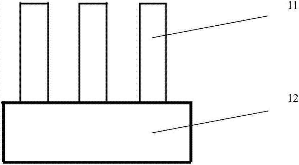
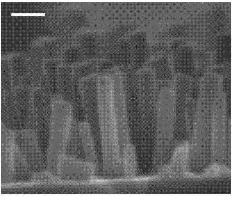
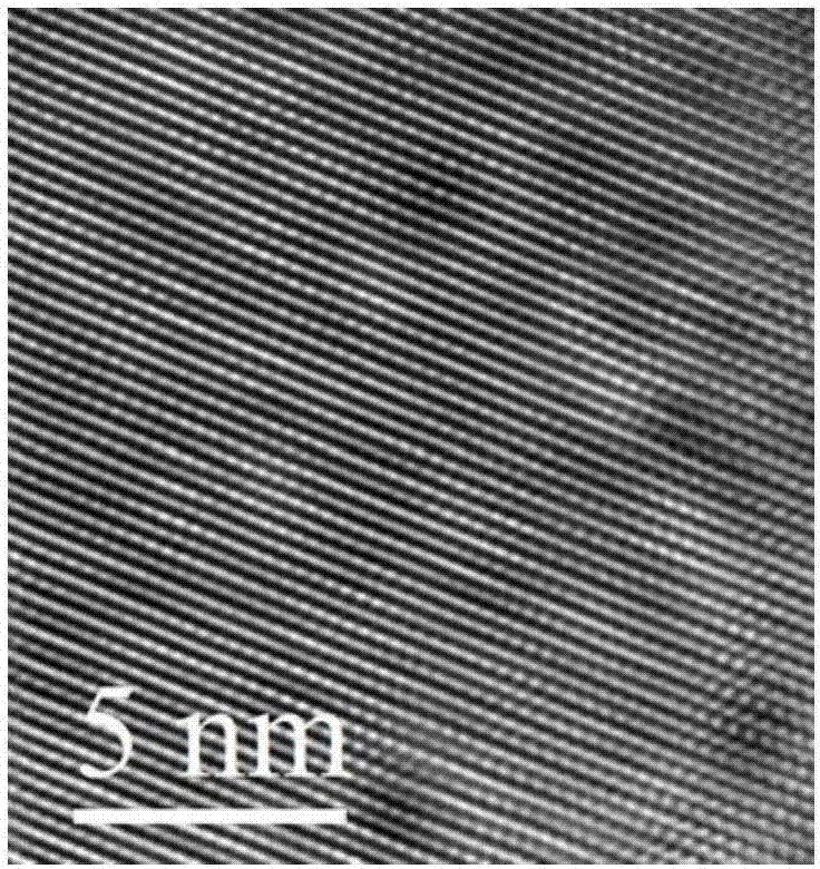
[0036] (1) Selection of the substrate and its crystal orientation: Si substrate is used, with the (111) plane as the epitaxial plane, and the crystal epitaxial orientation relationship is: the (0001) plane of GaN is parallel to the (111) plane of Si, that is, GaN ( 0001) / / Si(111), which is helpful for the epitaxial growth of high-quality GaN nanocolumns.

[0037] (2) Surface polishing of the substrate: Polish the surface of the Si substrate with diamond slurry, observe the surface of the substrate with an optical microscope until there are no scratches, and then perform polishing treatment by chemical mechanical polishing.

[0038] (3) Substrate cleaning: standard ultrasonic cleaning of the substrate with a mixture of HF and deionized water at a volume ratio of 1:10 for 1 minute, then repeated washing with deionized water for 1 minute, and finally drying with high-purity dry nitrogen .

[0039] (4) Substrate annealing treatment: transfer the cleaned and dried Si substrate to ...

Embodiment 2

[0044] (1) Selection of the substrate and its crystal orientation: Si substrate is used, with the (111) plane as the epitaxial plane, and the crystal epitaxial orientation relationship is: the (0001) plane of GaN is parallel to the (111) plane of Si, that is, GaN ( 0001) / / Si(111), which is helpful for the epitaxial growth of high-quality GaN nanocolumns.

[0045] (2) Surface polishing of the substrate: Polish the surface of the Si substrate with diamond slurry, observe the surface of the substrate with an optical microscope until there are no scratches, and then perform polishing treatment by chemical mechanical polishing.

[0046] (3) Substrate cleaning: standard ultrasonic cleaning of the substrate with a mixture of HF and deionized water at a volume ratio of 1:10 for 1 minute, then repeated washing with deionized water for 1 minute, and finally drying with high-purity dry nitrogen .

[0047](4) Substrate annealing treatment: transfer the cleaned and dried Si substrate to t...


PUM

PropertyMeasurementUnit
heightaaaaaaaaaa
diameteraaaaaaaaaa
heightaaaaaaaaaa

Abstract

The invention discloses a preparation method of a GaN nanometer column grown on an Si(111) substrate. The preparation method comprises the following steps: (1) selection of the substrate and crystal orientation thereof: adopting an Si substrate; (2) substrate cleaning; (3) substrate annealing treatment; (4) high-temperature growth of the GaN nanometer column: growing the GaN nanometer column under the condition of 900 to 1100 DEG C, wherein the growth time is 0.5 to 1.5 hours; and (5) low-temperature growth of the GaN nanometer column: growing the GaN nanometer column under the condition of 650 to 800 DEG C, wherein the growth time is 1.5 to 2.5 hours. The invention also discloses the GaN nanometer column grown on the Si(111) substrate obtained by the preparation method and application thereof. The non-uniformity of the nanometer column grown at high temperature is improved, the column disordered condition of the nanometer column grown at low temperature is also improved, and meanwhile the preparation method has the advantages of simple process, short production cycle and the like.

Description

technical field [0001] The invention relates to a GaN nano column, in particular to a GaN nano column grown on a Si (111) substrate, a preparation method and an application thereof. Background technique [0002] GaN and III-nitrides are widely used in light-emitting diodes (LEDs), lasers, and optoelectronic devices due to their advantages such as large band gap, stable physical and chemical properties, high thermal conductivity, and high electron saturation velocity. Compared with other wide-bandgap semiconductor materials, GaN materials not only have the above-mentioned advantages, but also their nanoscale GaN materials have more novel characteristics in terms of quantum effects, interface effects, volume effects, and size effects. [0003] GaN nanomaterials have a series of novel properties due to the "size effect", which makes it have great prospects in basic physical science and new technology applications, and has become a current research hotspot. The GaN nanocolumn s...

Claims


Application Information

Patent Timeline
Patent Type & Authority Applications(China)
IPC IPC(8): H01L33/20H01L33/22H01L33/00B82Y40/00
Inventor 李国强余粤锋高芳亮徐珍珠
Owner SOUTH CHINA UNIV OF TECH
Why Eureka
Try Eureka