Dual-layer polarization uncooled infrared detector structure and preparation method thereof

An uncooled infrared and detector technology, used in the manufacture of microstructure devices, microstructure technology, microstructure devices, etc., can solve the problems of complex optical components, complex optical path systems, and difficult design, and achieve obvious contour characteristics and simplification. Optical system, the effect of reducing difficulty

Active Publication Date: 2017-09-01
YANTAI RAYTRON TECH
View PDF9 Cites 12 Cited by
  • Summary
  • Abstract
  • Description
  • Claims
  • Application Information

AI Technical Summary

Problems solved by technology

[0005] In the existing polarization detection system, the polarization element is independent of the detector, and it is necessary to add a polarizer to the lens of the whole machine, or to design a polarization lens. This method is relatively expensive and difficult to design; The polarization information is obtained by rotating the polarization element. The disadvantages of this existing polarization detection system are: the optical elements are complicated, and the optical path system is complicated
In addition, the polarization image collected through the combination of polarizer and detector needs to be processed by image fusion algorithm, which is not only complicated but also relatively inaccurate

Method used


Image

  • Dual-layer polarization uncooled infrared detector structure and preparation method thereof
  • Dual-layer polarization uncooled infrared detector structure and preparation method thereof
  • Dual-layer polarization uncooled infrared detector structure and preparation method thereof

Examples


Embodiment 1

[0062] A method for preparing a double-layer polarization uncooled infrared detector structure, comprising the following steps:

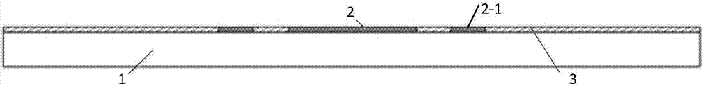
[0063] Step 1: Fabricate a metal reflective layer 2 on a semiconductor base 1 containing a readout circuit, and perform patterning on the metal reflective layer 2, and the patterned metal reflective layer 2 forms several metal blocks 2-1; the metal The block 2-1 is electrically connected to the readout circuit on the semiconductor base 1; then, an insulating dielectric layer 3 is deposited on the patterned metal reflective layer 2, and the insulating dielectric layer 3 is patterned to expose the metal block 2 -1, if figure 1 shown;

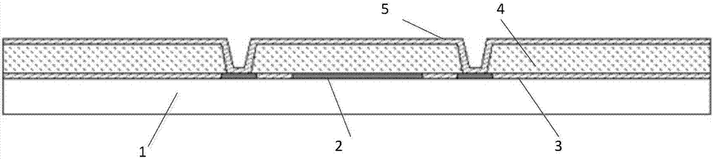
[0064] Step 2: Depositing a first sacrificial layer 4 on the insulating dielectric layer 3, and patterning the first sacrificial layer 4, depositing a first supporting layer 5 on the patterned first sacrificial layer 4, Such as figure 2 shown;

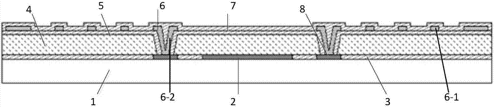
[0065] Step 3: Using photolithography and etching methods, etch away p...

Embodiment 2

[0075] The difference from Example 1 is that when the metal grating structure is prepared in step 10, the photoresist or PI is first spin-coated on the second support layer, and the grating pattern is obtained on the photoresist coating or PI coating by photolithography technology, The grating interval is 10-500nm, then, use physical vapor deposition or sputtering to deposit or sputter a metal film on the photoresist or PI coating that has been photoresisted, and finally, use the stripping process to remove the photoresist or PI coating, and Peel off excess metal film.


PUM

PropertyMeasurementUnit
Thicknessaaaaaaaaaa

Abstract

The invention relates to a dual-layer polarization uncooled infrared detector structure. The uncooled infrared detector structure comprises a semiconductor base and a detector body, wherein the detector body comprises an insulating medium layer, a metal reflecting layer, a first support layer, a metal electrode layer, a first protective layer, a second support layer, an electrode metal layer, a thermosensitive layer and a second protective layer; a first resonant cavity is formed between the first support layer and the insulating medium layer; a second resonant cavity is formed between the first protective layer and the second support layer; the thermosensitive layer is arranged on the electrode metal layer, and the dual-layer structure improves the infrared absorption efficiency of the pixel; a polarization structure is arranged on the second protective layer so as to realize the monolithic integration of a polarization sensitive type infrared detector, thereby greatly lowering the difficulty of the optical design; the invention further relates to a preparation method of the detector structure. The preparation method comprises a step of preparing the dual-layer uncooled infrared detector, and further comprises the step of preparing the polarization structure on the dual-layer uncooled infrared detector.

Description

technical field [0001] The invention belongs to the field of micro-electromechanical system process manufacturing in semiconductor technology, and in particular relates to a double-layer polarization uncooled infrared detector structure and a preparation method thereof. Background technique [0002] The unit of the uncooled infrared focal plane array detector usually adopts a cantilever beam micro-bridge structure, and the micro-bridge support structure is formed by using the sacrificial layer release process, and the heat-sensitive material on the support platform is connected to the substrate readout circuit through the micro-bridge. Now the requirements for the resolution of the detector are getting higher and higher, and the requirements for the array are getting bigger and bigger. If the size of the chip remains the same, the pixels will become smaller and smaller, and the requirements for the flatness of the pixels will be higher and higher; both sides The microbridge ...

Claims


Application Information

Patent Timeline
IPC IPC(8): B81B7/00B81B7/02B81C1/00G01J4/04G01J5/08G01J5/20
CPCG01J4/04G01J5/20B81B7/0009B81B7/02B81C1/00103B81C1/00476G01J2005/204G01J5/59
Inventor 邱栋杨水长王鹏王宏臣陈文礼
Owner YANTAI RAYTRON TECH
Why Eureka
Try Eureka