A kind of preparation method of silicon-based surface enhanced Raman substrate

A surface-enhanced Raman and substrate technology, applied in Raman scattering, instrumentation, vacuum evaporation coating, etc., can solve the problems of high cost and low price, and achieve the effect of low cost, easy operation and good repeatability

Inactive Publication Date: 2019-02-05
YUNNAN NORMAL UNIV
View PDF6 Cites 2 Cited by
  • Summary
  • Abstract
  • Description
  • Claims
  • Application Information

AI Technical Summary

Problems solved by technology

But it is expensive, so it is necessary to prepare a low-cost and stable monocrystalline silicon active substrate

Method used


Image

  • A kind of preparation method of silicon-based surface enhanced Raman substrate
  • A kind of preparation method of silicon-based surface enhanced Raman substrate
  • A kind of preparation method of silicon-based surface enhanced Raman substrate

Examples


Embodiment

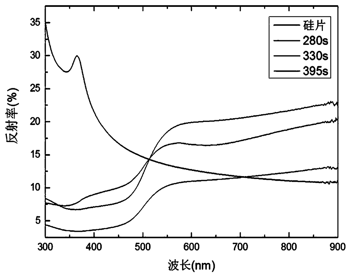
[0026] 1) First cut the single crystal silicon wafer p-type with a resistivity of 1-3Ω·cm into a size of 1.6cm×1.6cm for corrosion experiment, and pretreat the single crystal silicon before the reaction to remove surface impurities and oxidation things. Clean with a plasma cleaner for 10 minutes, put it into pure water and absolute ethanol successively for 5 minutes, soak in 4% HF for 60 seconds, then clean it with ultrapure water for 5 minutes, and dry it for later use. The resistivity of ultrapure water is 18.25 MΩ•cm;

[0027] 2) The configuration solubility is 10wt%K 2 CO 3 and 2wt%K 2 SiO 3 Solution, the temperature of the magnetic stirrer is set to 85 degrees Celsius, and when the temperature reaches the temperature, put the pretreated monocrystalline silicon into a closed container to react for 20 minutes. After the reaction is completed, use ultrapure water to repeatedly ultrasonically clean it, and dry it for later use;

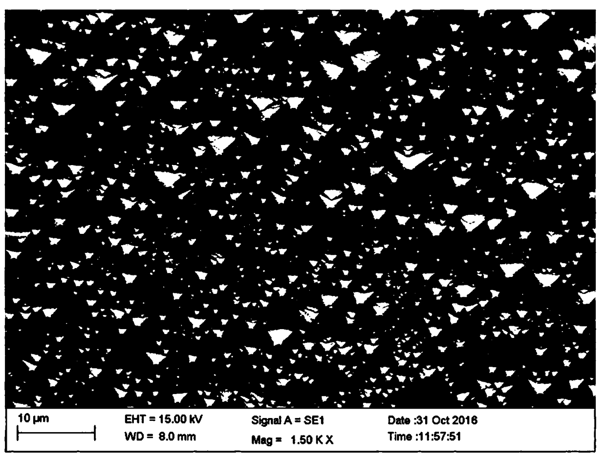
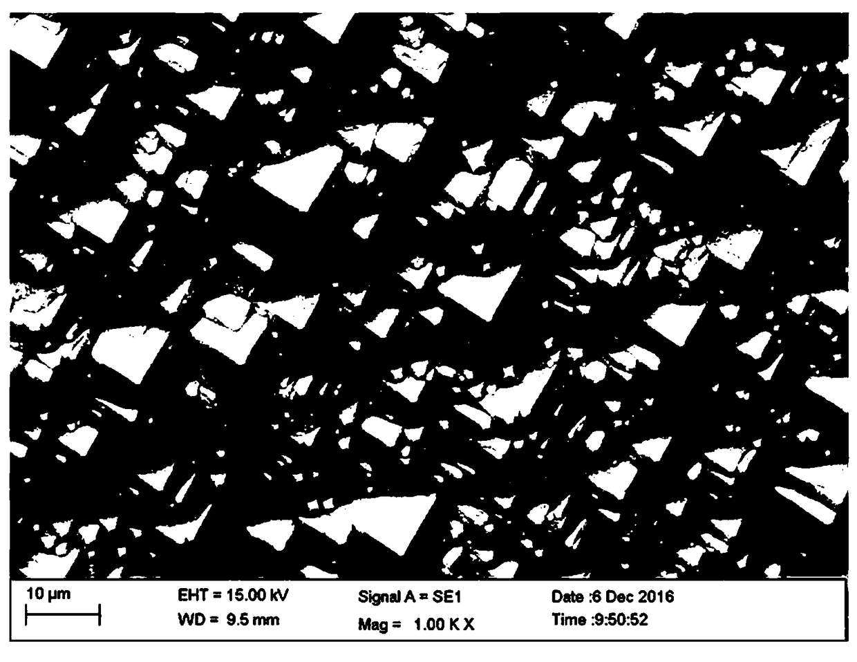
[0028] 3) Zeiss EVO MA15 scanning electr...


PUM

PropertyMeasurementUnit
diameteraaaaaaaaaa
thicknessaaaaaaaaaa
electrical resistivityaaaaaaaaaa

Abstract

The invention discloses a preparation method of a silicon-based surface-enhanced Raman substrate. Monocrystalline silicon acquires an ordered pyramid structure through a surface micro-structure preparation method, and the ordered pyramid is coated with a gold film. The preparation method comprises the steps that (1) the ordered pyramid structure on the surface of the monocrystalline silicon is obtained through corrosion of an alkaline solution; and (2) the surface of the monocrystalline silicon of the ordered pyramid structure is coated with the gold film with a certain thickness through an ion sputtering coating method. Composite nano particles obtained by the method have good chemical stability, substances with the concentration as low as 10-70 mol / L can be detected, and the absorption spectrogram obtained after long-time preservation hardly changes. The preparation method is easy and convenient to implement, low in cost, good in repeatability and capable of easily controlling the pyramid dimension and the thickness of the gold film.

Description

technical field [0001] The invention relates to a method for preparing a silicon-based surface-enhanced Raman substrate. Background technique [0002] Silicon is a very important semiconductor material that plays an important role in modern industry. The chemical and physical structure characteristics of the surface of silicon have aroused widespread interest not only in the disciplines of physics and chemistry, but also in nanomaterials, biomedicine and other disciplines. Recently, monocrystalline silicon has also been found to be widely used in the generation and deep processing of solar cells, the preparation of nanomaterials, biochemical sensors, integrated circuits, semiconductor separation devices, etc. This in turn established a higher requirement for silicon surface modification, leading to a new wave of research interest in silicon surface topographical features. [0003] Commonly used surface-enhanced Raman active substrates include electrochemically roughened el...

Claims


Application Information

Patent Timeline
Patent Type & Authority Patents(China)
IPC IPC(8): C23C14/02C23C14/16C23C14/34G01N21/65
CPCC23C14/021C23C14/165C23C14/34G01N21/658
Inventor 满石清叶巧云
Owner YUNNAN NORMAL UNIV
Why Eureka
Try Eureka