Non-polar surface quantum dot light-emitting diode and preparation method thereof
A quantum dot light-emitting, non-polar surface technology, applied in the direction of electrical components, circuits, semiconductor devices, etc., can solve the problems of high dislocation density in the active area, degradation of LEDs performance, and increased quality mismatch, so as to improve device efficiency , Eliminate the polarization effect, improve the effect of material quality
- Summary
- Abstract
- Description
- Claims
- Application Information
AI Technical Summary
Problems solved by technology
Method used
Image
Examples
preparation example Construction
[0052] The present invention also discloses a method for preparing the above-mentioned non-polar surface quantum dot light-emitting diode, which includes the following steps:
[0053] Step 1, sequentially forming a u-type GaN layer and an n-type GaN layer both on a non-polar surface on the substrate;
[0054] Step 2. First grow a wetting layer on the n-type GaN layer, then grow the non-polar InGaN quantum dots, and then grow the non-polar GaN barrier layer on the InGaN quantum dots; repeat the above steps n times to form active area;
[0055] Step 3, forming a p-type electron blocking layer and a p-type GaN layer both on the non-polar surface on the active region, and completing the preparation of the non-polar surface quantum dot light-emitting diode;
[0056] Among them, n is a natural number.
[0057] In some embodiments of the present invention, the value range of the above n is 3≤n≤15.
[0058] In some embodiments of the present invention, the formation environment of ...
Embodiment 1
[0065] This embodiment provides a non-polar surface quantum dot light-emitting diode structure, which includes the main structure from bottom to top:
[0066] A substrate, the substrate is a (1-102) R-plane sapphire plane or a PSS substrate, and can also be a silicon, silicon carbide, lithium aluminate or GaN homogeneous substrate;
[0067] A stress covariant layer, which is fabricated on the substrate, can be formed by annealing one or more sets of InGaN flexible layers and GaN buffer layers, and has a porous or stripe-like morphology, which can be used to control the growth of GaN on it Layer stress state, other materials that can be made into porous or stripe-like morphology, such as InN, ZnO, AlN or carbon nanorods, can be used as materials for the stress-covariant layer;
[0068] An undoped GaN layer on the non-polar surface, which is fabricated on the stress covariant layer, and the stress state is controlled by the stress covariant layer below it;
[0069] A non-polar ...
Embodiment 2
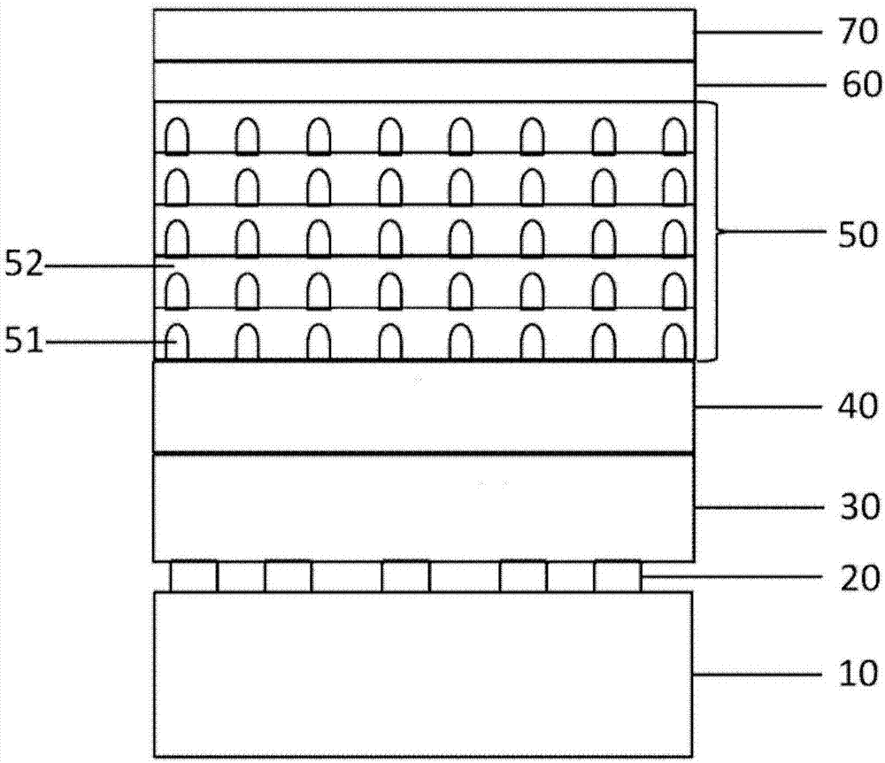
[0084] Such as figure 1 As shown, the present embodiment provides a non-polar surface quantum dot light-emitting diode, including:
[0085] A substrate 10, the substrate 10 is an R-face sapphire substrate of the (1-102) face;
[0086] It should be noted that this embodiment uses a sapphire substrate. For other substrates, such as silicon, silicon carbide or lithium aluminate, as long as the lattice matching degree with the non-polar A-plane GaN is less than 20%, can also be used;
[0087] A stress covariant layer 20 formed by annealing the InGaN flexible layer and the GaN buffer layer, which is fabricated on the substrate 10 . Among them, the thickness of the InGaN flexible layer is 20-100nm, the thickness of the GaN buffer layer is 30-150nm, and the stress-covariant layer formed by annealing has a stripe-like morphology, which can be used to control the stress state of the GaN layer grown on it;
[0088] A non-polar undoped GaN layer 30 is fabricated on the stress-conformi...
PUM
| Property | Measurement | Unit |
|---|---|---|
| Diameter | aaaaa | aaaaa |
| Height | aaaaa | aaaaa |
| Thickness | aaaaa | aaaaa |
Abstract
Description
Claims
Application Information


