Transmission electron microscope in-situ nanomechanical tensile testing sample bonding method

A technology of transmission electron microscopy and tensile testing, which is applied in the preparation of test samples, testing the strength of materials by applying stable tension/pressure, and analyzing materials by measuring secondary emissions. The device cannot be reused and the cost is high, so as to achieve the effect of low cost

CN107219243AInactive Publication Date: 2017-09-29DALIAN UNIV OF TECH
5 Cites 15 Cited by

Patent Information

Authority / Receiving Office
CN · China
Current Assignee / Owner
Publication Date
2017-09-29
Estimated Expiration
Not applicable · inactive patent

Smart Images

  • Figure 1
    Figure 1
  • Figure 2
    Figure 2
  • Figure 3
    Figure 3
Patent Text Reader

Abstract

The invention relates to a transmission electron microscope in-situ nanomechanical tensile testing sample bonding method, which uses a developed micromechanical unit to transfer a sample under an optical microscope and uses epoxy resin to fix the sample. A counterweight, cantilevers and operating tools are fixedly bonded by using epoxy resin, and a three-coordinate micromotion platform of the optical microscope is adopted as a moving unit; the ultrasonically dispersed sample is transferred into a spray unit, and a spraying method is adopted to uniformly spray the sample onto a copper net; the micromechanical unit is used for transferring a single sample onto a drawing unit of an in-situ nanomechanical testing system under the optical microscope; the second-stage operating tool of the micromechanical unit dips epoxy resin and transfer the epoxy resin to the bonded part of the sample, and the sample bonded by the epoxy resin is kept still under room temperature for 24 hours for solidification. The transmission electron microscope in-situ nanomechanical tensile testing sample bonding method provided by the invention is simple, low-cost and nondestructive, and a transmission electron microscope in-situ nanomechanical tensile testing method for one-dimensional nanomaterials is achieved.
Need to check novelty before this filing date? Find Prior Art

Description

technical field

[0001] The invention relates to a method for bonding samples for in-situ nanomechanical tensile testing by transmission electron microscopy, which relates to the field of in-situ nanomechanical testing by transmission electron microscopy, and in particular to in-situ nanomechanical tensile testing of one-dimensional nanomaterials. Background technique

[0002] Silicon is widely used in semiconductors, microelectronics, optoelectronics, solar cells and other fields due to its abundant reserves, non-toxicity, and excellent photoelectric properties. Silicon carbide has a wide range of applications in high temperature, high pressure, high frequency, radiation-resistant semiconductor devices and ultraviolet detectors. With the development of science and technology, high-performance equipment requires high-performance parts to have nano-level flatness and sub-nanometer roughness. Therefore, nano-precision manufacturing methods must be used for high-performance sili...

Examples

Embodiment

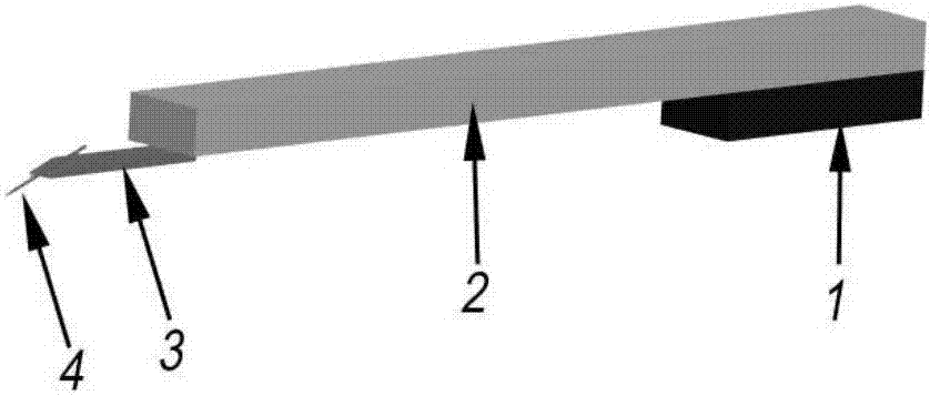
[0035] Fabricate micromechanical manipulation devices capable of micro-movement under an optical microscope, such as figure 1 As shown, the micro-mechanical moving device uses the three-coordinate micro-moving platform of another optical microscope, and the cantilever beam is made of plastic. The length of the cantilever beam is 2-2.5cm, the width is 9-10mm, and the height is 3.5-4mm. The counterweight is made of glass block, and the weight is 30-35g. The first-level operation tool is a stainless steel needle or toothpick, and the tip curvature radius is 0.1-0.2mm; the second-level operation tool is hair, and the tip curvature radius is 10-15μm. Fix with epoxy glue.

[0036] Put the 300-mesh micro-grid used in the preparation of the transmission electron microscope sample into alcohol for ultrasonic cleaning for 20-30 minutes, so that the supporting film of the micro-grid or ultra-thin micro-grid is removed, and the copper grid remains.

[0037] The sample is a Beta-type SiC...