Impedance transformer network circuit structure
A network circuit and impedance transformation technology, applied in impedance matching network, multi-terminal pair network, etc., can solve the problems of large leakage current of diode, small junction capacitance of diode, view and so on.
- Summary
- Abstract
- Description
- Claims
- Application Information
AI Technical Summary
Problems solved by technology
Method used
Image

Examples
Embodiment Construction
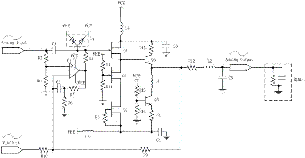
[0037] The present invention provides an impedance transformation network circuit structure, using three JFET tubes cascaded to form a source follower, using two transistors cascaded to form a buffer, which can reduce the difference between the input capacitance of the source follower and the output capacitance of the buffer At the same time, increase the bandwidth, reduce external interference, increase the isolation between channels, and suppress the generation of high-frequency oscillation.
[0038] see below figure 1 , an embodiment of an impedance transformation network circuit structure provided by the present invention, including:
[0039] The input signal (AnaLog) is divided into two paths, the first branch transmits high-frequency signals, and the second branch transmits low-frequency signals.
[0040] The second branch from the input signal (Analog) is connected to the gate of the first JFET tube (Q1) through the first capacitor (C1); then it is amplified by the fir...
PUM
 Abstract
Description
Claims
Application Information