Composite transparent conductive film and preparation method thereof

A transparent conductive film, transparent conductive technology, applied in the direction of equipment for manufacturing conductive/semiconductive layers, cable/conductor manufacturing, conductive layers on insulating carriers, etc., can solve the problem of unfavorable large-scale patterning of thin films Improve performance, affect carrier injection and other issues, achieve enhanced conductivity and electrical stability, strong corrosion resistance, and good conductivity

Active Publication Date: 2017-10-20
SOUTH CHINA UNIV OF TECH
View PDF4 Cites 3 Cited by
  • Summary
  • Abstract
  • Description
  • Claims
  • Application Information

AI Technical Summary

Problems solved by technology

In terms of printing preparation, Au is difficult to achieve transparency, mainly because it is difficult to accurately control the thickness of the film below 30nm. Secondly, there are many other impurities in the film, which reduces the light transmittance. In addition, the Au electrode due to the work function Higher, non-ohmic contacts are formed with most oxide semiconductors, which affects carrier injection and is not conducive to the improvement of device performance
[0005] The Au film prepared by evaporation or magnetron sputtering method has high quality, good electrical conductivity and stable chemical properties. film or photolithography to achieve patterning, which is not conducive to the large-scale patterning of thin films

Method used


Image

  • Composite transparent conductive film and preparation method thereof
  • Composite transparent conductive film and preparation method thereof
  • Composite transparent conductive film and preparation method thereof

Examples


Embodiment 1

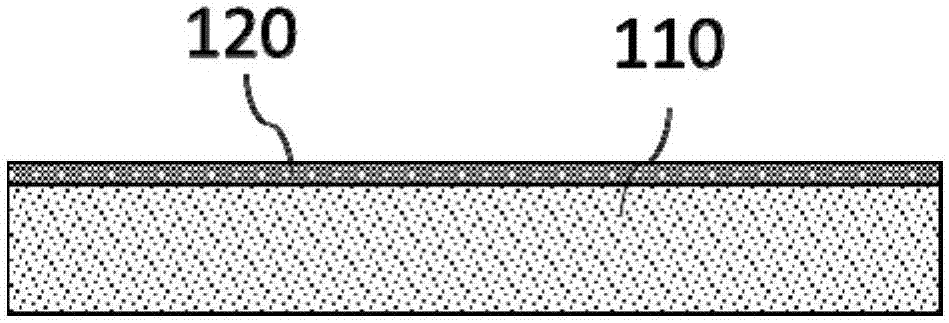
[0033] A composite transparent conductive film, which is composed of a transparent oxide layer and a thin metal layer stacked, wherein the thin metal layer is located under the transparent oxide layer, the thickness of the thin metal layer is 3-30nm, the thin metal layer is in a transparent state, and the thin metal layer Nanopores are present in the layer; during the preparation of the transparent oxide layer, the transparent conductive oxide is able to penetrate through the nanopores and come into contact with the substrate.

[0034] The concrete preparation method of this composite transparent conductive film is:

[0035] In step (1), one or more thin metal layers are prepared by coating or vacuum coating without patterning the prepared thin metal layers.

[0036] Among them, the thickness of the thin metal layer is controlled within 30nm. On the one hand, the metal film is in a transparent state; of adhesion. In addition, it can also avoid the peeling off of the whole pi...

Embodiment 2

[0047] A patterned ITO / Au composite transparent conductive film was prepared and used as an electrode.

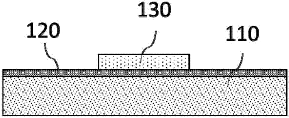
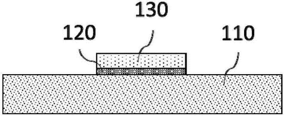
[0048] Such as figure 1 As shown, firstly, a layer of Au thin film 120 with a thickness of 10 nm is deposited on a glass substrate 110 . Next, if figure 2 As shown, after the Au film is treated with plasma for 5 minutes, ITO ink is directly inkjet printed on it. The atomic number ratio of Sn and In is 10 / 90 to form an ITO precursor film pattern 130, and the precursor pattern is annealed at 350°C for 1 hour. Finally, an ITO transparent conductive oxide film pattern with a line width of 70 μm and a thickness of 30 nm is formed. Thereafter, the entire film was placed in water for ultrasonic treatment for 2 min, and then dried with nitrogen to obtain the following: image 3 For the composite transparent conductive film shown, the square resistance of the film is

[0049] The composite transparent conductive film has low resistivity and good conductivity, and is suitabl...

Embodiment 3

[0051] Fabrication of patterned AZO / Pt composite transparent electrodes.

[0052] Such as figure 1 As shown, first a layer of Pt film 120 with a thickness of 8 nm is evaporated on the glass substrate 110, and then, as figure 2 As shown, after the Pt film is treated with UV for 5 minutes, AZO ink is directly ink-jet printed on it, wherein the ratio of the atomic number of Al to Zn is 3 / 97, forming an AZO precursor film pattern 130, and the precursor pattern is annealed at 350°C After 1 hour, an AZO transparent conductive oxide film pattern with a line width of 80 μm and a thickness of 40 nm was formed. Thereafter, the entire film was put into an aqueous hydrogen peroxide solution for ultrasonication for 3 min, and then dried with nitrogen to obtain the following: image 3 For the composite transparent conductive film shown, the square resistance of the film is

[0053] The composite transparent conductive film has low resistivity and good conductivity, and is suitable for...


PUM

PropertyMeasurementUnit
thicknessaaaaaaaaaa
thicknessaaaaaaaaaa
thicknessaaaaaaaaaa

Abstract

The present invention discloses a composite transparent conductive film and a preparation method thereof. The composite transparent conductive film is formed by stacking a transparent oxide layer and a thin metal layer, wherein the thin metal layer is located under the transparent oxide layer, the thickness of the thin metal layer is 3-30nm, the thin metal layer is in a transparent state, and the thin metal layer has nanopores. The preparation method comprises: the step (1), preparing the thin metal layer; the step (2), preparing the transparent oxide layer to form a required pattern, putting the required pattern into liquid after annealing processing to remove the thin metal layer which is not covered by the transparent oxide layer, storing the transparent oxide layer and the thin metal layer which is covered by the transparent oxide layer, and realizing the patterning of the composite transparent conductive film. The patterning process does not need photo-mask lithography, the prepared composite transparent conductive film is good in resistivity and good in electricity stability, has a certain optical transmissibility, and is heat resisting, antioxidant and erosion-resistant.

Description

technical field [0001] The invention relates to the technical field of conductive films, in particular to a conductive oxide / metal composite transparent conductive film and a patterning method thereof, which can be used in electrode wiring. Background technique [0002] In recent years, transparent oxide conductive thin films, such as ITO, AZO, IZO, FTO, ATO, etc., have been widely used in optoelectronic devices, such as touch screens, electrochromic devices, solar cells, organic light-emitting diodes, and thin-film transistors. [0003] At present, most of the industrialized transparent oxide conductive films are prepared by physical vapor deposition method, and mask or traditional photolithography method is also used to realize the patterning of the film, which not only causes waste of materials, but also complicates the preparation process, resulting in The cost is relatively high. Inkjet printing, as a solution processing technology that can directly achieve patterned d...

Claims


Application Information

Patent Timeline
Patent Type & Authority Applications(China)
IPC IPC(8): H01B13/00H01B13/22H01B5/14H01L29/423B82Y30/00
CPCB82Y30/00H01B5/14H01B13/0026H01B13/22H01L29/42384
Inventor 兰林锋彭俊彪李育智
Owner SOUTH CHINA UNIV OF TECH
Why Eureka
Try Eureka