Manufacturing method for hard micro-fluid chip

A technology of microfluidic chips and manufacturing methods, applied in the direction of applying stable tension/pressure to test material strength, material inspection products, instruments, etc., can solve problems such as not being able to chip

Active Publication Date: 2017-10-31
TSINGHUA UNIV +1
View PDF7 Cites 12 Cited by
  • Summary
  • Abstract
  • Description
  • Claims
  • Application Information

AI Technical Summary

Problems solved by technology

Among them, after oxygen plasma treatment, hydroxyl nano-layers will be produced on the surfaces of both sides, and the two will be sealed through hydrogen bonds. This process is simple to operate and only takes a few minutes to complete the sealing process, but it is only suitable for the packaging of PDMS soft materials; Chemical modif

Method used


Image

  • Manufacturing method for hard micro-fluid chip
  • Manufacturing method for hard micro-fluid chip
  • Manufacturing method for hard micro-fluid chip

Examples


Embodiment 1

[0073] Embodiment 1, making epoxy resin microfluidic chip (substrate material is PDMS)

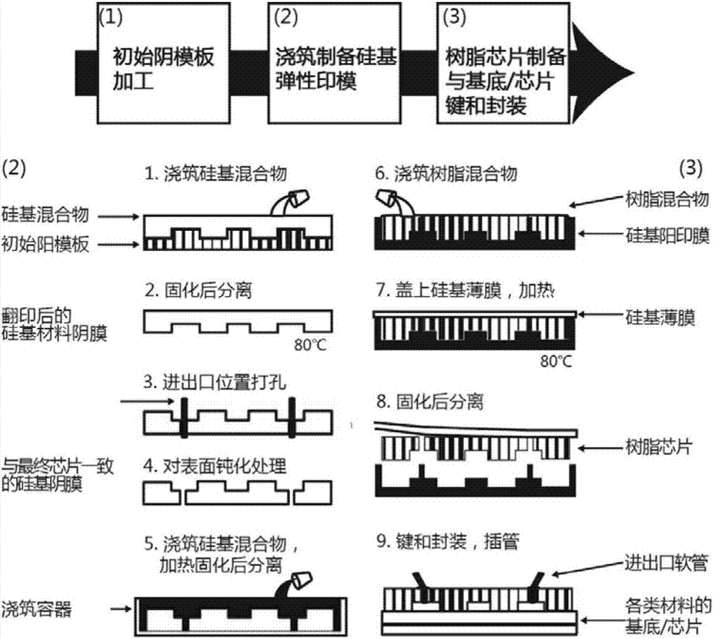
[0074] like figure 1 As shown, the microfluidic chip was fabricated according to the following steps:

[0075] (1) PDMS prepolymer and curing agent are mixed at a volume ratio of 10:1, and the mixture after removing air bubbles is poured onto a template / mold, which is a male master mold (such as a silicon wafer) containing a convex microchannel structure. SU-8 convex mold formed by photolithography).

[0076] (2) After the mold poured with the PDMS mixture in step (1) is dried at 80 degrees for 1 hour, the flash is removed and cleaned to become a microfluidic chip to be copied, which is a PDMS microfluidic chip corresponding to the concave microstructure chip.

[0077] (3) Use a hole puncher to punch through holes of appropriate size, such as 0.1mm, 0.2mm, 0.3mm, 0.4mm, etc., at the position of the sample inlet and outlet on the PDMS chip.

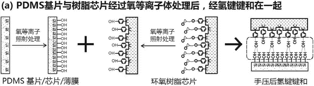
[0078] (4) Passivate the perforated PDMS chi...

Embodiment 2

[0086] Embodiment 2, making epoxy resin microfluidic chip (substrate material is PMMA)

[0087] like Figure 4 As shown, the microfluidic chip was fabricated according to the following steps:

[0088] (1) PDMS prepolymer and curing agent are mixed at a volume ratio of 10:1, and the mixture after removing air bubbles is poured onto the template / mold, which is a female master mold containing a concave micro-channel structure (such as laser engraving machine-cut PC material). Engraving can cut through holes of appropriate size at the position of the sample inlet and outlet on the female master mold at the same time, such as 0.1mm, 0.2mm, 0.3mm, 0.4mm, etc.

[0089] (2) After the mold poured with the PDMS mixture in step (1) is heated at 80 degrees for 1 hour, it is peeled off and cut off the flash, and cleaned to prepare a positive PDMS mold that is opposite to the pattern of the template / mold but contains micropillars entering and exiting the sample hole. The chip is a mold w...

Embodiment 3

[0096] Embodiment 3, making epoxy resin microfluidic chip (substrate material is glass)

[0097] An epoxy resin microfluidic chip was prepared according to the steps in Example 2, only the substrate in step 9) was replaced with a glass substrate. In this embodiment, the XPS energy spectrum scanning result is as follows Figure 7 as shown, Figure 7 The upper two curves are the surface XPS scanning results of amino unmodified glass (samples 1 and 2), and the middle two curves are the surface XPS scanning results of amino modified glass (samples 3 and 4), where The peak of N element near the 401eV energy level increases significantly after modification, indicating that there is indeed an increase of amino groups on the glass surface after modification. Therefore by Figure 7 It can be seen that the amino groups are successfully modified on the surface of the glass substrate in this example.

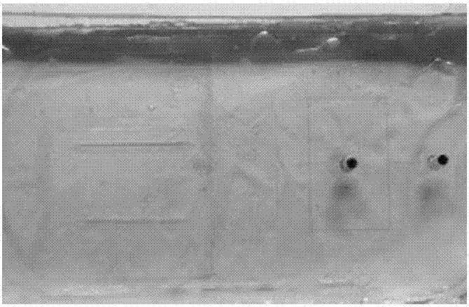
[0098] In the present embodiment, the photograph of the epoxy resin chip that prepa...


PUM


Abstract

The invention discloses a manufacturing method for a hard micro-fluid chip. The manufacturing method comprises the following steps: preparing an upper chip and chemically bonding and packaging the upper chip under a semi-cured state with a substrate, thereby acquiring the hard micro-fluid chip. The upper chip can be prepared from epoxy resin or amino resin; when the upper chip is prepared, the heating curing temperature is 45-85 DEG C and the time is 15 minutes to 8 hours; a thermal polymerized epoxy resin material is used after the two materials of prepolymer and curing agent are mixed, the viscosity thereof after mixing is low (approximate to mineral oil viscosity), the rolling printing for a tiny structure at micron scale and even nanometer scale is convenient and the rolling precision is high; the mixture can be solidified within 40min under the temperature of 80 DEG C, the preparation time of the micro-fluid chip is shortened, the period is short, the consumption of a reagent is less and the batch production is convenient; the hard micro-fluid chip can be flexibly packaged and combined with various substrates; the packaging is independent of external high temperature and high pressure environments; and the packaging strength is high and the speed is high.

Description

technical field [0001] The invention relates to a manufacturing method of a hard microfluidic chip. Background technique [0002] Microfluidics, also known as Lab-on-a-chip, refers to the integration of basic operating units such as sample preparation, reaction, separation, and detection involved in the fields of biology, chemical medical analysis, etc. Or a type of technology that is basically integrated into a chip whose core unit is a micron size, and automatically completes the whole process of analysis. Its goal is to integrate the functions of the entire laboratory and biological laboratory, including sampling, dilution, reagent addition, reaction, separation, detection and sample transfer, etc. on the microchip, shorten operation time and labor consumption, and improve detection sensitivity and accuracy. rate and repetition rate, exploring new areas and applications of science. Due to its great potential in the fields of biology, chemistry, and medicine, it has deve...

Claims


Application Information

Patent Timeline
IPC IPC(8): G01N35/00G01N3/08G01N21/59G01N21/64G01N33/48
CPCG01N3/08G01N21/59G01N21/64G01N33/48G01N35/00029G01N2021/6419G01N2035/00158G01N2035/00168G01N2203/0003G01N2203/0017G01N2203/0067G01N2203/0075
Inventor 刘鹏程振李彩霞孙敬
Owner TSINGHUA UNIV
Why Eureka
Try Eureka