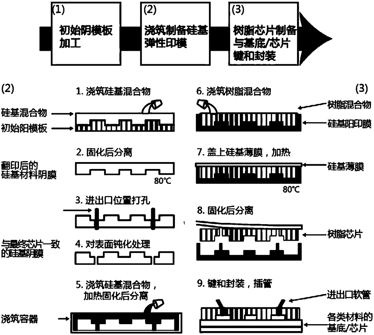
A kind of fabrication method of rigid microfluidic chip
A technology of microfluidic chip and manufacturing method, which is applied in the direction of applying stable tension/pressure to test the strength of materials, fluorescence/phosphorescence, instruments, etc., and can solve problems such as incapability of chips
- Summary
- Abstract
- Description
- Claims
- Application Information
AI Technical Summary
Problems solved by technology
Method used
Image
Examples
Embodiment 1
[0073] Embodiment 1, making epoxy resin microfluidic chip (substrate material is PDMS)
[0074] Such as figure 1 As shown, the microfluidic chip was fabricated according to the following steps:
[0075] (1) PDMS prepolymer and curing agent are mixed at a volume ratio of 10:1, and the mixture after removing air bubbles is poured onto a template / mold, which is a male master mold (such as a silicon wafer) containing a convex microchannel structure. SU-8 convex mold formed by photolithography).
[0076] (2) After the mold poured with the PDMS mixture in step (1) is dried at 80 degrees for 1 hour, the flash is removed and cleaned to become a microfluidic chip to be copied, which is a PDMS microfluidic chip corresponding to the concave microstructure chip.
[0077] (3) Use a hole puncher to punch through holes of appropriate size, such as 0.1mm, 0.2mm, 0.3mm, 0.4mm, etc., at the position of the sample inlet and outlet on the PDMS chip.
[0078] (4) Passivate the perforated PDMS ...
Embodiment 2
[0086] Embodiment 2, making epoxy resin microfluidic chip (substrate material is PMMA)
[0087] Such as Figure 4 As shown, the microfluidic chip was fabricated according to the following steps:
[0088] (1) PDMS prepolymer and curing agent are mixed at a volume ratio of 10:1, and the mixture after removing air bubbles is poured onto the template / mold, which is a female master mold containing a concave micro-channel structure (such as laser engraving machine-cut PC material). Engraving can cut through holes of appropriate size at the position of the sample inlet and outlet on the female master mold at the same time, such as 0.1mm, 0.2mm, 0.3mm, 0.4mm, etc.
[0089] (2) After the mold poured with the PDMS mixture in step (1) is heated at 80 degrees for 1 hour, it is peeled off and cut off the flash, and cleaned to prepare a positive PDMS mold that is opposite to the pattern of the template / mold but contains micropillars entering and exiting the sample hole. The chip is a mol...
Embodiment 3
[0096] Embodiment 3, making epoxy resin microfluidic chip (substrate material is glass)
[0097] An epoxy resin microfluidic chip was prepared according to the steps in Example 2, only the substrate in step 9) was replaced with a glass substrate. In this embodiment, the XPS energy spectrum scanning result is as follows Figure 7 as shown, Figure 7 The upper two curves are the surface XPS scanning results of amino unmodified glass (samples 1 and 2), and the middle two curves are the surface XPS scanning results of amino modified glass (samples 3 and 4), where The peak of N element near the 401eV energy level increases significantly after modification, indicating that there is indeed an increase of amino groups on the glass surface after modification. Therefore by Figure 7 It can be seen that the amino groups are successfully modified on the surface of the glass substrate in this example.
[0098] In the present embodiment, the photograph of the epoxy resin chip that prepa...
PUM
| Property | Measurement | Unit |
|---|---|---|
| transmittivity | aaaaa | aaaaa |
Abstract
Description
Claims
Application Information


