
A trench junction barrier Schottky diode and its manufacturing method

A junction barrier Schottky technology and a fabrication method, which are applied to trench junction barrier Schottky diodes and their fabrication fields, can solve problems such as electric field aggregation and breakdown, eliminate electric field breakdown and improve withstand voltage characteristics , the effect of increasing the main junction area

Active Publication Date: 2020-03-06
INST OF MICROELECTRONICS CHINESE ACAD OF SCI
View PDF5 Cites 0 Cited by
  • Summary
  • Abstract
  • Description
  • Claims
  • Application Information

AI Technical Summary

Problems solved by technology

[0006] The trench junction barrier Schottky diode and its manufacturing method provided by the present invention can solve the problem that the traditional main junction structure is easy to cause electric field accumulation in the prior art, and effectively eliminate the problem that the main junction is prone to electric field breakdown

Method used


Image

  • A trench junction barrier Schottky diode and its manufacturing method
  • A trench junction barrier Schottky diode and its manufacturing method
  • A trench junction barrier Schottky diode and its manufacturing method

Examples


Embodiment Construction

[0028] In order to make the purpose, technical solutions and advantages of the embodiments of the present invention clearer, the technical solutions in the embodiments of the present invention will be clearly and completely described below in conjunction with the drawings in the embodiments of the present invention. Obviously, the described embodiments It is only some embodiments of the present invention, but not all embodiments. Based on the embodiments of the present invention, all other embodiments obtained by persons of ordinary skill in the art without making creative efforts belong to the protection scope of the present invention.

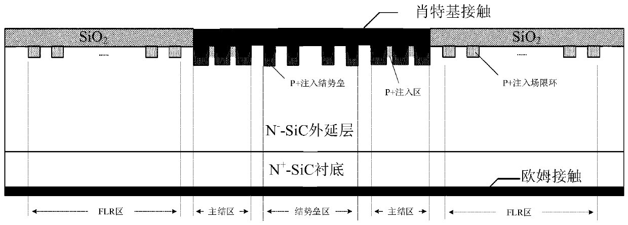
[0029] In a first aspect, the present invention provides a trench junction barrier Schottky diode. In one embodiment of the present invention, a silicon carbide (SiC) trench junction barrier Schottky diode is provided.

[0030] figure 1 A schematic cross-sectional structure diagram of a SiC trench junction barrier Schottky diode according t...


PUM


Abstract

The present invention provides a trench junction barrier Schottky diode and a manufacturing method thereof. The method comprises: the step 1, providing a substrate configured to manufacture a device, wherein an epitaxial layer is grown at the right side of the substrate; the step 2, manufacturing a field limiting ring area and a preparation main junction area on the epitaxial layer, wherein the preparation main junction area is configured to provide first ion implantation; the step 3, etching a junction barrier groove on the epitaxial layer except the field limiting ring area, wherein the main junction groove is etched at the preparation main junction area, and the junction barrier groove and the junction groove are subjected to second ion implantation; the step 4, manufacturing ohmic contact at the back of the substrate; the step 5, manufacturing a passivation layer and Schottky contact at the right side of the device; and the step 6, manufacturing a metal electrode at the right side of the device and performing passivation. The present invention further provides a trench junction barrier Schottky diode. The trench junction barrier Schottky diode and the manufacturing method thereof can reduce the main junction electric field aggregation effect while effectively shielding the Schottky surface electric field, vertically increase the main junction area and improve the pressure-resisting features.

Description

technical field [0001] The invention relates to the technical field of semiconductor devices, in particular to a trench junction barrier Schottky diode and a manufacturing method thereof. Background technique [0002] Modern technology has continuously put forward higher requirements for the volume, reliability, withstand voltage and power consumption of semiconductor power devices. With the shrinking of the transistor feature size, due to the short channel effect and other physical laws and the limitation of production cost, the mainstream silicon-based materials and CMOS technology are developing to the 10nm process node and it is difficult to continue to improve. Silicon carbide has a larger band gap than silicon, and has a higher doping concentration and a smaller epitaxial layer thickness than silicon power devices of the same withstand voltage level, so the forward conduction resistance can be greatly reduced and the power loss is large At the same time, silicon carbi...

Claims


Application Information

Patent Timeline
Patent Type & Authority Patents(China)
IPC IPC(8): H01L21/329H01L29/872
CPCH01L29/6606H01L29/8725
Inventor 董升旭汤益丹白云申华军杨成樾
Owner INST OF MICROELECTRONICS CHINESE ACAD OF SCI
Learn More