Epitaxial wafer of light-emitting diode and preparation method thereof

A technology of light-emitting diodes and epitaxial wafers, which is applied in the direction of electrical components, circuits, semiconductor devices, etc., can solve the problems of reducing the internal quantum efficiency of light-emitting diodes, reducing the radiation recombination of electrons and holes, increasing the stress and defects of the light-emitting layer, and achieving Avoid too high forward voltage, improve internal quantum efficiency, and reduce the effects of lattice defects

Active Publication Date: 2017-11-07
HC SEMITEK ZHEJIANG CO LTD
View PDF5 Cites 18 Cited by
  • Summary
  • Abstract
  • Description
  • Claims
  • Application Information

AI Technical Summary

Problems solved by technology

[0005] GaN and the substrate are heterogeneous materials, and the lattice mismatch is large, which causes stress and defects during the growth of the epitaxial wafer. The stress and defects extend to the light-emitting layer along the lamination direction of the epitaxial wafer. In addition, the InGaN quantum well layer and There is also a lattice mismatch between the GaN quantum barrier layers, which will further increase the stress and defects in the light-emitting layer, resulting in non-radiative recombination between electrons and holes, thus reducing the radiative recombination of electrons and holes, and ultimately reducing Internal Quantum Efficiency of Light Emitting Diodes

Method used


Image

  • Epitaxial wafer of light-emitting diode and preparation method thereof
  • Epitaxial wafer of light-emitting diode and preparation method thereof
  • Epitaxial wafer of light-emitting diode and preparation method thereof

Examples


Embodiment 1

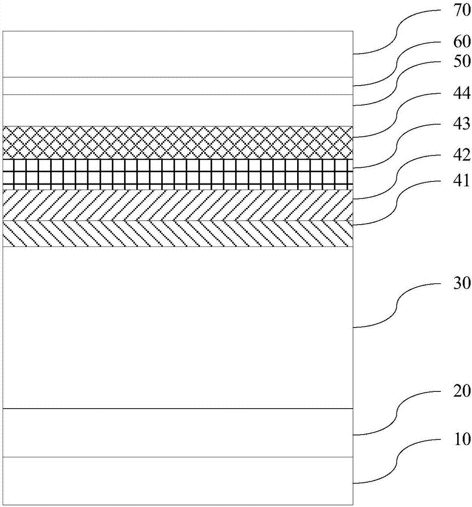
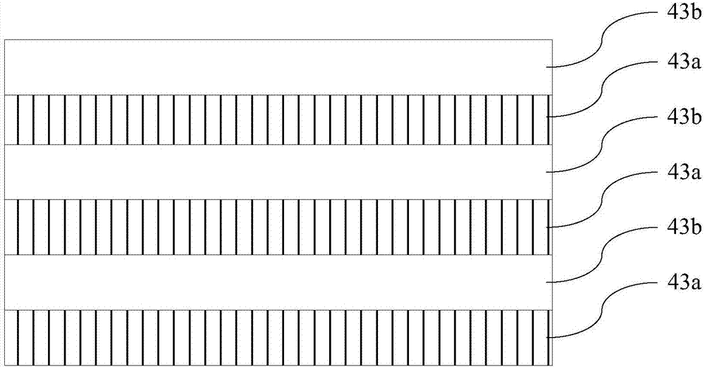
[0029] An embodiment of the present invention provides an epitaxial wafer of a light emitting diode, see figure 1 , the epitaxial wafer includes a substrate 10 and a buffer layer 20, an undoped gallium nitride layer 30, a defect barrier layer 41, a first stress release layer 42, a second stress release layer 43, a first Three stress release layers 44 , an N-type GaN layer 50 , a multi-quantum well layer 60 and a P-type GaN layer 70 .

[0030] In this example, if figure 1 As shown, the buffer layer 20 is stacked on the substrate 10, the undoped gallium nitride layer 30 is stacked on the buffer layer 20, the defect barrier layer 41 is stacked on the undoped gallium nitride layer 30, and the first stress release layer 42 stacked on the defect barrier layer 41, the second stress release layer 43 is stacked on the first stress release layer 42, the third stress release layer 44 is stacked on the second stress release layer 43, and the N-type gallium nitride layer 50 is stacked on ...

Embodiment 2

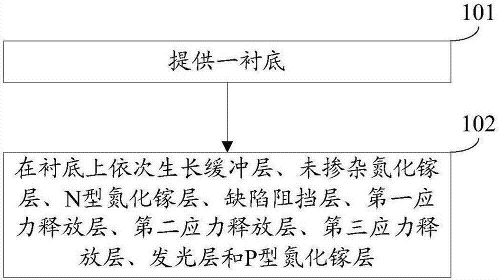
[0047] An embodiment of the present invention provides a method for preparing an epitaxial wafer of a light-emitting diode, which is suitable for preparing the epitaxial wafer provided in Example 1. See image 3 , the preparation method comprises:

[0048] Step 101: Provide a substrate.

[0049] In a specific implementation, the substrate will be annealed in a hydrogen atmosphere first, and then the temperature will be controlled at 1050° C. to 1180° C., and the nitriding treatment will be performed for 10 minutes to clean the substrate surface.

[0050] Step 102: sequentially grow a buffer layer, an undoped GaN layer, an N-type GaN layer, a defect barrier layer, a first stress release layer, a second stress release layer, a third stress release layer, and a light emitting layer on the substrate layer and the P-type GaN layer.

[0051] In this embodiment, the defect blocking layer is a silicon-doped aluminum gallium nitride layer, the first stress release layer is a silicon-...

Embodiment 3

[0071] An embodiment of the present invention provides a method for preparing an epitaxial wafer of a light-emitting diode, and the preparation method provided in this embodiment is a specific realization of the preparation method provided in Embodiment 3. Specifically, see Figure 4 , the preparation method comprises:

[0072] Step 201: Provide a sapphire substrate.

[0073] Step 202: Control the growth temperature to 575° C. and the growth pressure to 500 torr, and grow a gallium nitride layer with a thickness of 30 nm on the sapphire substrate to form a buffer layer.

[0074] Step 203: Control the growth temperature to 1100° C. and the growth pressure to 405 torr, and grow an undoped gallium nitride layer with a thickness of 1.25 μm on the nucleation layer.

[0075] Step 204: Control the growth temperature to 1100° C. and the growth pressure to 405 torr, and grow an N-type GaN layer with a thickness of 1.9 μm on the undoped GaN layer.

[0076] Step 205: Control the growt...


PUM

PropertyMeasurementUnit
thicknessaaaaaaaaaa
thicknessaaaaaaaaaa
thicknessaaaaaaaaaa

Abstract

The invention discloses an epitaxial wafer of a light-emitting diode and a preparation method thereof, and belongs to the technical field of semiconductors. The epitaxial wafer comprises a substrate, a buffer layer, an undoped gallium nitride layer, an N-type gallium nitride layer, a defect blocking layer, a first stress release layer, a second stress release layer, a third stress release layer, a light emitting layer and a P-type gallium nitride layer, and is characterized in that the buffer layer, the undoped gallium nitride layer, the N-type gallium nitride layer, the defect blocking layer, the first stress release layer, the second stress release layer, the third stress release layer, the light emitting layer and the P-type gallium nitride layer are sequentially laminated on the substrate, the defect blocking layer is a silicon-doped aluminum gallium nitride layer, the first stress release layer is a silicon-doped gallium nitride layer, the second stress release layer comprises a plurality of first sub-layers and a plurality of second sub-layers which are arranged in an alternately laminating manner, the first sub-layers are undoped InGaN layers, the second sub-layers are silicon-doped gallium nitride layers, and the third stress release layer is a silicon-doped InGaN layer; and the doping concentration of silicon in the defect blocking layer is lower than that of the first stress release layer, the doping concentration of silicon in the first stress release layer is higher than that of each second sub-layer, and the doping concentration of silicon in each second sub-layer is lower than that of the third stress release layer. The light emitting efficiency can be improved according to the invention.

Description

technical field [0001] The invention relates to the technical field of semiconductors, in particular to an epitaxial wafer of a light emitting diode and a preparation method thereof. Background technique [0002] A light-emitting diode (English: Light Emitting Diode, referred to as: LED) is a semiconductor electronic component that can emit light. Semiconductor light-emitting diodes represented by gallium nitride (GaN) have excellent characteristics such as large band gap, high electron saturation drift velocity, high temperature resistance, and high power capacity, and have broad prospects in the emerging optoelectronic industry. The chip is the most important part of the LED, and the epitaxial wafer is the raw material for chip preparation. [0003] Existing GaN-based LED epitaxial wafers are formed by epitaxially growing U-type GaN layers, N-type GaN layers, light-emitting layers, and P-type GaN layers on heterogeneous substrates (such as sapphire substrates). Among the...

Claims


Application Information

Patent Timeline
Patent Type & Authority Applications(China)
IPC IPC(8): H01L33/12H01L33/32H01L33/00
CPCH01L33/0075H01L33/12H01L33/32H01L33/325
Inventor 刘华容万林胡家辉
Owner HC SEMITEK ZHEJIANG CO LTD
Why Eureka
Try Eureka