Automatic test platform of high-speed ADC chip and software framework design method thereof

An automatic test and chip technology, applied in the direction of electronic circuit testing, measuring electricity, measuring devices, etc., can solve the problem of short time-consuming test process, and achieve the effect of reliable high-speed data signal transmission and high test rate.

Active Publication Date: 2017-11-24
苏州迅芯微电子有限公司
View PDF7 Cites 42 Cited by
  • Summary
  • Abstract
  • Description
  • Claims
  • Application Information

AI Technical Summary

Problems solved by technology

It can achieve a certain degree of rapid and automated testing of a large number of chips, but the testing scheme based on this equipment has many limitations, especially for high-speed ADC chips. The test accuracy of the static characteristics and dynamic characteristic parameters of the chip under test needs to provide adjustable frequency amplitude or high-precision analog input signal; for the data of the data output interface of the high-speed ADC chip under test, the processing core needs

Method used


Image

  • Automatic test platform of high-speed ADC chip and software framework design method thereof
  • Automatic test platform of high-speed ADC chip and software framework design method thereof
  • Automatic test platform of high-speed ADC chip and software framework design method thereof

Examples


Embodiment Construction

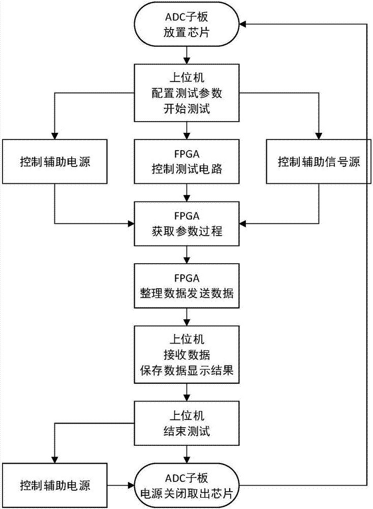
[0066] The technical solutions described in the present invention will be clearly and completely described below in conjunction with an embodiment of the present invention and the accompanying drawings. Apparently, the described embodiment is only a part of the embodiments of the present invention, not all of them. Based on the embodiments of the present invention, all other embodiments obtained by persons of ordinary skill in the art without making creative efforts belong to the protection scope of the present invention.

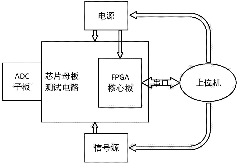
[0067] see figure 1 As shown, the automatic test platform of a kind of high-speed ADC chip of the present invention is made up of five parts: ADC sub-board, test motherboard, FPGA core board, host computer and test equipment.

[0068] The ADC sub-board includes the ADC chip placement test socket, the basic working circuit of the chip and the chip interface that leads out. The device for placing the ADC chip is used to replace the ADC chip. After testing on...


PUM


Abstract

The invention discloses an automatic test platform of a high-speed ADC chip and a software framework design method thereof. The design method comprises the steps of step 1, FPGA underlying logic drive design: the FPGA underlying logic part completes construction of the hardware foundation, including realizing underlying logic control, foundation computation and soft core hardware configuration of the hardware module; and synchronous drive algorithm design including the tested high-speed ADC, calibration algorithm design, hardware drive design of the onboard high-precision ADC/DAC and register array and hardware FFT operation; step 2, test parameter acquisition: the FPGA soft core receives an upper computer command to control the test process and transmits the command to the FPGA hardware program to drive an external circuit to acquire data so as to obtain the test parameter value by applying the processing algorithm, wherein the test parameters are mainly divided into static parameters and dynamic parameters; and step 3, upper computer program design. The high-precision level characteristic and the high-speed data characteristic of the chip can be simultaneously measured, and "one-key acquisition" can be realized through programming control.

Description

technical field [0001] The invention belongs to the technical field of testing integrated circuit chips, and in particular relates to an automatic testing platform applied to high-speed analog-to-digital converter chips and a software structure design method thereof. Background technique [0002] High-speed ADC chips (analog-to-digital converters) are widely used in the fields of radar, optical communication, software radio and mobile communication. With the continuous improvement of the conversion rate and sampling accuracy of ADC chips, the test tasks of a large number of chips after mass production are heavy and very important, and higher requirements are placed on the existing test system; the test tasks include testing various types of ADC chips. Characteristic parameters: static characteristics, dynamic characteristics, data\clock output characteristics and power consumption characteristics, etc. [0003] At present, mass production testing of chips in the field of ch...

Claims


Application Information

Patent Timeline
IPC IPC(8): G01R31/28
CPCG01R31/2856
Inventor 王潜
Owner 苏州迅芯微电子有限公司
Why Eureka
Try Eureka